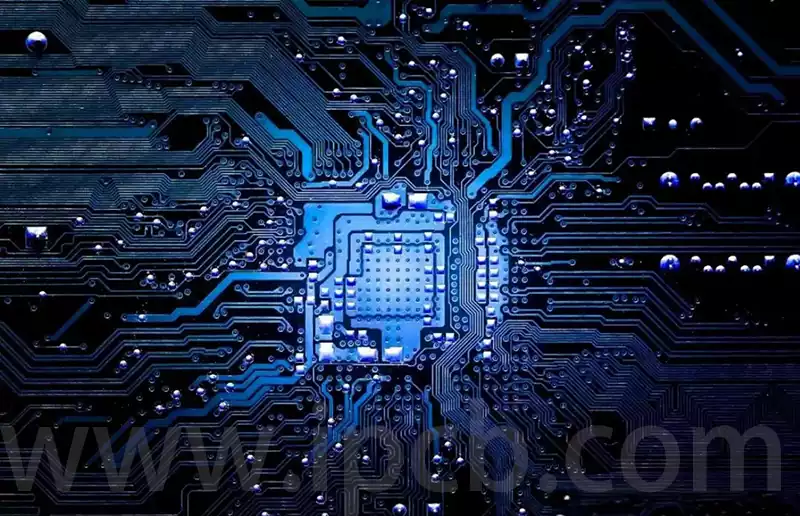
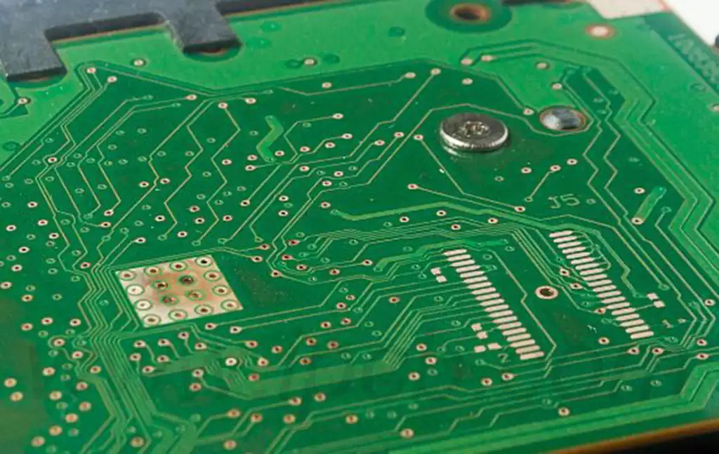
pcb wire soldering is the process of soldering on a printed circuit board. The process involves connecting wires or other components to the pcb, usually by heating the solder to make the connection. Soldering on a pcb requires a great deal of care and precision to ensure that the solder joints are strong and reliable and do not damage the rest of the board. pcb wires play a very important role in the manufacture and repair of electronic devices as they provide a strong and reliable connection.
Soldering is a process also known as “joining”. It is the process of melting a metal alloy and pressing it into a joint between two other metals. The molten metal flows into the gap and cools to form a strong bond. Solder is a metal alloy that melts at low temperatures and is bonded to the flow surface between them. As the solder cools and hardens, it forms a strong bond between the parts being joined.
Why solder wires in pcb? There are several important reasons for soldering wires in pcb:
- Provide electrical connection: Soldering wires can connect different components, conductors and electronics to the pcb, thus providing a good electrical connection between the parts.
- mechanical fixation: by soldering, it ensures that the wires are firmly fixed to the pcb, preventing them from loosening or breaking when the equipment is moved or vibrated.
- Space saving: Compared to using sockets or other connectors to connect wires, soldering allows for more efficient use of space and can reduce the size of the assembled part.
- Increased reliability: Soldering provides a durable and reliable connection that is less susceptible to external interference or damage, and ensures that signal transmission and functional performance are supported in a stable and reliable manner.
pcb soldering materials
Many different types of solder exist on the market and choosing the best type of solder can seem like a daunting task for a new designer or assembler. Solder creates an electrical connection between metal contacts by causing the molten solder (a soft alloy) to form a eutectic and melt on cooling. The metal mixture that makes up the soldered pcb will determine its mechanical strength after solidification, the required melting temperature, and any fumes produced during the soldering process. We can distinguish between types of pcb soldering materials by core material, metal content and flux type.
Metal content
Leaded solder mixtures are known as soft solder and were the beginning of the electronics industry. It has a melting point of about 180-190°C and a shelf life of about 2 years. Common leaded solder alloys include:
60/40 tin/lead;/37 tin/lead; 2/36/2 tin/lead/silver
Other tin/lead ratios include 50/50, 30/70, and 10/90. tin is primarily used as a base metal because it gives the alloy a lower melting point, while lead inhibits the growth of tin whiskers. Higher tin concentrations ensure higher shear and tensile strength of soldered joints.The silver component of 62/36/2 Sn/Pb/Ag provides lower contact resistance and corrosion resistance. Note that there are other types of solder (indium, zinc alloys, etc.), but these are not used for pcb because they are not compatible with the pcb manufacturing process.
Lead-free solders have become increasingly popular since the EU adopted the Restriction of Hazardous Substances (RoHS) directive limiting the use of lead in electronic products. One problem with lead-free solders is that they are more prone to the formation of tin whiskers. Conformal coatings are often used to prevent the formation of these tin whiskers and provide protection against moisture and corrosion.
Lead free pcb solder wire is sold in single rolls with a reducing agent in the core. This reducing agent (which I will discuss below) removes any oxide film from the metal contacts to ensure that the electrical contact is highly conductive. If hand soldering is used, the type of material contained in the core is another issue to consider.
Solder core material
The spool of solder or solder paste will contain one of the following types of material to flux the metal contacts during the soldering process:
Organic acid-based flux: An acid-based flux ensures that oxides are effectively removed from the metal contacts during soldering. This type of flux is water-soluble and needs to be cleaned of residue after soldering to prevent corrosion.
Rosin-based fluxes: Rosin is a solid resin derived from coniferous trees. Rosin-based flux residues do not cause corrosion, so it can be used when organic acid-based flux residues are more difficult to remove.
Solid Core: Some wires have a solid core and do not contain any flux, so flux needs to be applied by hand. As long as the flux is available, this type of solder can be used for manual soldering.
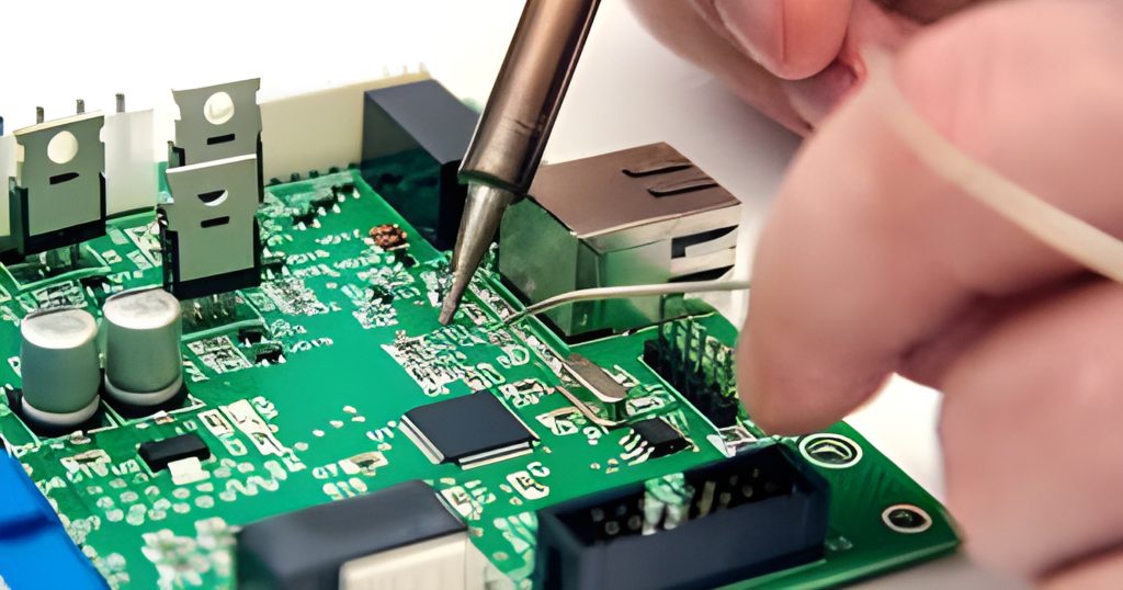
Second, the circuit board welding precautions
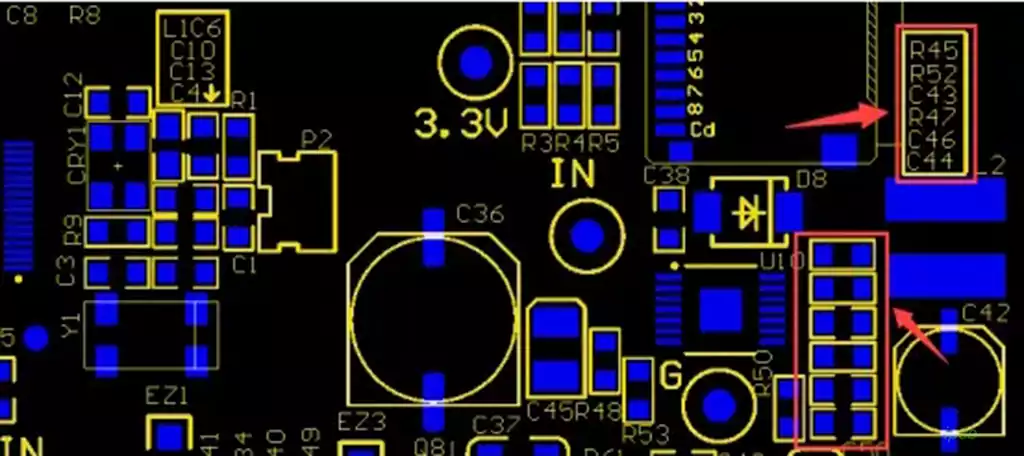
- Remind everyone to get the pcb bare board should first be checked for appearance, to see if there are short circuits, circuit breakers and other issues, and then familiarize yourself with the development board schematic diagram, the schematic diagram and the pcb silkscreen layer to avoid schematic diagrams and pcb does not match.
- pcb welding materials required to prepare complete, should be classified components, according to the size of all components into several categories, to facilitate subsequent welding. Need to print a complete list of materials. In the welding process, not welded one, then the corresponding options with a pen to cross out, so as to facilitate subsequent welding operations.
- Welding should be taken before wearing a static ring and other anti-static measures to avoid static damage to the components. Welding equipment required to ensure that the soldering iron tip is clean and tidy after complete preparation. Recommended for the first time to choose a flat angle soldering iron, such as 0603 type package components such as soldering iron can better contact the pad, easy to weld. Of course, for experts, this is not a problem.
- Select components for welding, should be in accordance with the components from low to high, from small to large order for welding. So as not to weld the larger components to the welding of smaller components to bring inconvenience. Priority welding integrated circuit chips.
- Before welding the integrated circuit chip to ensure that the chip is placed in the correct direction. For the chip silkscreen layer, the general rectangular pad indicates the beginning of the pin. Welding should be fixed first chip a pin, the position of the components for fine-tuning after fixing the chip diagonal pins, so that the components are accurately connected to the position after welding.
- SMD ceramic capacitors, voltage regulator circuit regulator diodes without positive and negative points, light-emitting diodes, tantalum capacitors and electrolytic capacitors need to distinguish between positive and negative. For capacitors and diode components, generally have a significant identification of the end should be negative. In the SMD LED package, along the direction of the light for the positive – negative direction. For silkscreen marking for the diode circuit diagram package components, there is a vertical line should be placed at the negative end of the diode.
- For the crystal, passive crystal oscillator generally only two pins, and no positive and negative points. Active crystal oscillator generally have four pins, need to pay attention to the definition of each pin to avoid welding errors.
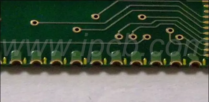
- For plug-in components welding, such as power module-related components, the device pins can be modified before welding. After the components are placed and fixed, generally on the back through the soldering iron will melt the solder by the pad into the front. Solder does not have to put too much, but first of all should make the components stable.
- Soldering process should be recorded in a timely manner found in the pcb design issues, such as installation interference, pad size design is not correct, component packaging errors, etc., in order to prepare for subsequent improvements.
- After welding should use a magnifying glass to view the solder joints, check whether there is a virtual weld and short circuit and so on.
- After the completion of the circuit board welding work, alcohol and other cleaning agents should be used to clean the surface of the circuit board to prevent the circuit board surface attached to the iron filings so that the circuit short-circuit, but also to make the circuit board more clean and beautiful.
10 tips for soldering
- pcb must have a clean surface.
- pcb soldering wire size must match the size of the soldering.
- Use a soldering iron tip that matches the components to be soldered.
- Select the solder and flux carefully.
- Select a soldering temperature hot enough to melt the solder effectively, but not too hot.
- Hold the tip of the soldering iron over the leads and contacts/pad until both are up to temperature.
- Wipe enough solder to cover the contact pads and surround the leads.
- If necessary, trim the leads with sharp wire cutters, not to the solder joints.
- Remove flux residue from the soldered area with a good quality flux remover.
pcb soldering wires play a vital role in electronic equipment, its role and function involves connecting circuits, transmitting signals and supplying energy and other aspects.
- connecting circuits: one of the main roles of pcb soldering wires is to connect different components to create a complete circuit. On a pcb, individual components are connected by soldering wires, pins, slots and other components to form a complete functional module or system. This connection is especially important in modern electronic devices because it ensures a stable and reliable signal transmission path between the various parts.
- Transmission of signals: In addition to simply establishing physical connectivity, solder wires are also responsible for transmitting and carrying various types of signals. These signals, which can be digital/analog signals from sensors, communication devices, or other control components, are guided through the wires to the exact location where they need to go. At the same time, in high-speed data transmission applications, high quality and properly laid out and designed solder can greatly enhance the quality of the data path.
- Energy supply: In addition, in some cases, there is a need for energy to be delivered directly from the pcb to specific areas or components. For example, in power amplifiers, DC-DC converters, and other applications there will be a need, and these needs to be achieved through the precise and effective placement of the appropriate solder joints.
- Enhancement of structural strength: Another noteworthy feature is the reinforcement of the structural support between the pcb material and other parts (e.g., metal chassis). When assembled, reasonable and secure arrangement of pcb solder joints can significantly improve the overall product mechanical reliability and vibration and shock resistance.
- Improve heat dissipation: Finally, there is a very important but often overlooked mission – to help dissipate heat! Good design and use of the right size filler helps to quickly transport heat from the pcb to the final destination for dispersion.
Soldering is one of the most important steps in PCB manufacturing. To ensure soldering quality and reliability, it is important to use the proper pcb soldering wire materials and tools and to follow the correct soldering procedure. The quality and reliability of the board can be ensured by cleaning the surface of the board, winding the solder wire, heating the solder joints, removing the soldering iron, inspecting the solder joints and cleaning the surface.