General rules of pcb layout, in pcb design, simple pcb layout refers to the planning of how to place electronic components on printed circuits and the process of placing electronic components in pcb design, including planning and placement of the two stages. Reasonable layout is the first step to the success of the pcb design, the layout of the results of the good and bad will directly affect the pcb wiring and manufacturability, inappropriate layout may lead to the failure of the entire pcb design or production efficiency is very low. In the pcb design on how to reasonable layout should consider the manufacturability of the pcb, reasonable wiring requirements, the unique characteristics of a certain electronic product.
Manufacturability of pcb and layout design
The manufacturability of the pcb refers to the design of the pcb to meet the production conditions of electronic products, if it is a test product or production volume is not large enough to require manual production, can be less consideration; if you need to mass production, the need for production line production of products, then the pcb layout should be carefully planned, in the layout of the layout to determine the rules of the design of your pcb board.
When starting a new printed circuit board design, it is sometimes easy to forget the important design rules that govern the project. If some simple clearances can be determined early in the design, a lot of component shifting and rewiring can be avoided later. So where can that information be obtained?
The first place to start is with the pcb design rules manufacturer. Good manufacturers usually publish their features online or will provide this information in their documentation. If it is not apparent on their website, send them an e-mail and ask about their features. It’s best to perform this before you start laying out components. In the meantime, be sure to submit your proposed overlay for review or find their standard overlay data and put it to work.
Once you have found the list of features, you should compare it to any industry reliability standards you will be using (Level 2 vs. Level 3, or specialty standards). After determining these points, you should select more conservative design layout constraints to ensure manufacturability and reliability, and you can code these into the board design rules.
Consider the process requirements of the mounter, plug-in machine and the layout requirements of different soldering methods in production, and strictly follow the requirements of the production process, which is the first thing that should be considered in the design of mass-produced pcb. The actual size of the pcb, the location of the positioning components, etc., coincide with the structural element diagram of the process, and the layout of components in the areas where there are requirements for limiting the height of the components meets the requirements of the structural element diagram.
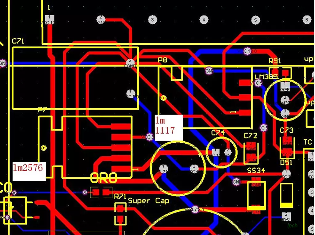
Component layout spacing meets the assembly requirements: surface mount components greater than 20mil, IC greater than 80mil, BGA greater than 200mi. no small components between high components, height greater than 10mm components within 5mm of the placement of SMD components and small inserted components.
The pin spacing, component direction, component spacing, and component library of the components to be processed by wave soldering should be considered as the process requirements of wave soldering. When wave soldering is used, try to ensure that both ends of the component’s solder joints touch the solder wave at the same time. When the size difference between the sheet components arranged next to each other and the spacing is very small, the smaller components in the wave soldering should be arranged in front, to avoid the larger size of the components behind the smaller size of the components obscured, resulting in leakage of welding. Circuit boards of different components adjacent to the pads between the minimum distance between the graphics should be more than 1mm, then a simple pcb layout is particularly important.
During the layout process, board design rules will help you avoid most design errors that can lead to manufacturing and assembly problems. After setting up the board design rules, you can start the layout process.
Fine-tuning Component Arrangement
The component placement phase of the pcb layout design process is both an art and a science that requires strategic consideration of the major spaces available on the pcb. The goal of component placement is to create a board that can be easily routed. Ideally, the fewer layer transitions the better. Additionally, the design rules must be met and the necessary component placement must be satisfied. These points can be difficult to balance, but a simple process can help board designers meet these requirements:
- Place the required components first. Often there are components that must be placed in specific locations, sometimes due to mechanical enclosure constraints or due to their size. It is best to place these components and lock them in place before proceeding with the rest of the layout.
- Place large processors and ICs Components such as high pin count ICs or processors often need to be connected to multiple components in the design. Placing these components in a centralized location makes it easier to route traces in the pcb layout.
- Try to avoid crossing networks. Unwired networks are often visible when components are placed in a pcb layout. Please minimize the number of network crossings. Each network crossing requires a layer transition through a vias. If network crossings can be avoided with the help of creative component placement, then a simple pcb layout will be realized.
- SMD pcb board design rules. It is recommended that all surface mount device (SMD) components be placed on the same side of the board. The main reason for this is that each side of the board requires its own solder lines along the SMD during assembly, so placing all SMDs on one side will help you avoid some additional assembly costs.
- Try reorientation. You can rotate components to try to avoid network crossings. Try orienting the connected pads so that they face each other, which can help simplify wiring.
Place the power, ground, and signal traces. After placing the components, you can route the power, ground, and signal traces to ensure that the signals have a clean and trouble-free transmission path. Keep the following guidelines in mind during this stage of the layout process:
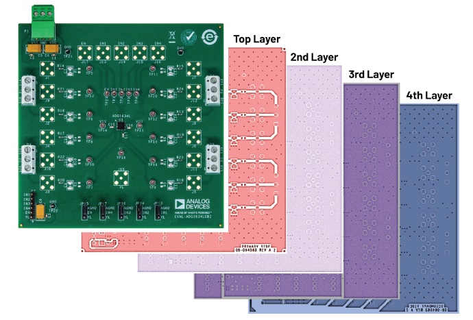
Placement of Power and Ground Layers
Typically, power and ground should be placed on both internal layers. For 2-layer boards, this may not be easy, so you may want to place a large ground plane on one layer and then route signal and power traces on another. For 4-layer board stacks and higher, you should use a ground plane instead of trying to route ground traces. For components that require direct power connections, if a power plane is not used, it is recommended to use a common rail for each power supply, making sure that the traces are wide enough (100 mils is sufficient if 5 to 10A) and that the power traces are not connected between parts.
Some recommendations state that the plane layer arrangement must be symmetrical, but this is not a strict requirement for manufacturing. In large boards this may be necessary to minimize the possibility of distortion, but in smaller boards this is not an issue. Focus first on power and ground access and make sure that all traces have strong return path coupling to the nearest ground plane, then consider perfect symmetry in the pcb design stack.
Wiring guidelines for pcb layout
Next, connect the signal traces to match the network in the schematic. pcb layout best practices suggest that short, direct traces should always be placed between components whenever possible, although this may not always be practical on larger boards. If the component arrangement forces horizontal trace routing on one side of the board, the traces should always be routed vertically on the other side. This is one of many important 2 layer pcb board design rules.
As the number of layers in a stack increases, printed circuit board design rules and simple pcb layout guidelines become more complex. Your wiring strategy will require alternating horizontal and vertical traces in the layers unless a reference plane is used to separate each signal layer. In very complex boards for specialized applications, many of the often touted pcb best practices may no longer apply and you will need to follow application-specific pcb board design guidelines.
A pcb layout design uses traces to connect components, but how wide should these traces be? The trace width required for different networks depends on three possible factors:
Manufacturability. The traces should not be too thin for reliable manufacturing. In most cases, the trace width you use will be much larger than the minimum a manufacturer can produce.
Current. The current carried in the trace will determine the minimum width needed to prevent the trace from overheating. At higher currents, the trace will need to be wider.
Impedance. High speed digital or RF signals require a specific trace width to achieve the required impedance value. This does not apply to all signals or networks, so you do not need to implement impedance controls for each network in your board design rules.
Hot air pads are a simple pcb layout design feature that may be needed to ensure that the board remains manufacturable during wave soldering, or in other words, for through-hole components that are directly attached to a flat surface. It is difficult to maintain process temperatures when soldering through-holes directly to solder joints on flat surfaces, so hot air pads are recommended to ensure that soldering temperatures remain constant. The principle of hot air pads is simple: slowing down the rate at which heat is dissipated into the plane during the soldering process will help prevent cold connections.
When routing analog and digital devices that require these types of capacitors, it is necessary to connect a bypass capacitor close to the power supply pins, usually 0.1 µF. Keep the pins as short as possible to reduce the inductive reactance of the trace and to be as close to the device as possible.
Adding bypass or decoupling capacitors to a board, and the placement of these capacitors on the board, is basic common sense for both digital and analog designs, but their functions are different.
In analog wiring design bypass capacitors are often used to bypass high frequency signals on the power supply, which may enter sensitive analog chips through the power supply pins if bypass capacitors are not added. Generally, these high-frequency signals have frequencies that exceed the ability of the analog device to suppress them.
If bypass capacitors are not used in analog circuits, noise may be introduced into the signal path, or in more serious cases, even vibration. For digital devices like controllers and processors, decoupling capacitors are also needed, but for different reasons.
One of the functions of these capacitors is to act as a “miniature” charge reservoir, this is because in digital circuits, the execution of gate state switching (i.e., switching switching) usually requires a large amount of current, when switching switching transient currents are generated on the chip and flow through the circuit board, it is advantageous to have this extra “spare” charge. It is advantageous to have this extra “spare” charge.
If there is not enough charge to perform the switching action, it can cause the supply voltage to change significantly. Too large a change in voltage can cause the digital signal levels to go into an indeterminate state and will likely cause the state machine in the digital device to operate incorrectly.
Simple pcb layouts can be challenging. Proper management of board layers and development of proper grounding schemes are also among the key points that system designers must consider when striving to achieve optimal performance in mixed-signal system layouts. Developing a component floor plan will help establish the overall integrity of the system design. Properly organizing the board layers will help manage current and signals throughout the board. Finally, selecting the most favorable grounding scheme will improve system performance and prevent problems associated with high noise signals and return currents.