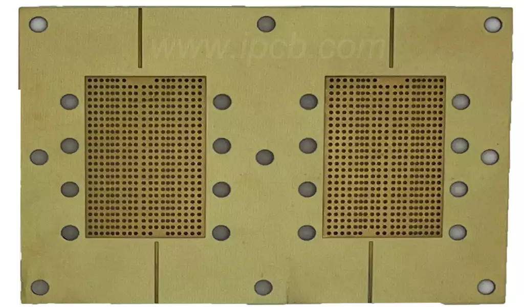
PCB side plating, also known as pcb edge plating, is a copper plating that is applied from the top to the bottom surface of the board and along (at least) one of the peripheral edges. PCB edge plating is the process of allowing a metallised layer to extend up to the edge of the board and wrap around to the other side, creating a continuous metallic coating. This technique is primarily used to build complete Faraday cages to prevent Electromagnetic Interference (EMI) leakage, to protect circuits from external interference or to reduce the impact on neighbouring circuits.PCB Side Edge Plating passes through the PCB for a strong connection and reduces the likelihood of device failures, especially for small PCBs and motherboards.Examples of this plating are commonly found in Wi-Fi and Bluetooth modules. During the manufacturing process, the edges to be metallised should be milled prior to the copper plating process. Appropriate surface treatment is applied to the PCB edges after copper deposition.
Design rules for pcb edge plating
The plating is required not only to encapsulate the edge of the board, but also to wrap around the surface of the board. The minimum distance required for the plating to wrap to the surface is 0.015’.Requires wrapping of the interior finish and attachment of the plating to the edge. Also detailed is the minimum distance from the board surface features to the wrap-to-surface plating (0.010‘), as well as the distance required for adjacent wiring features (0.100’).
The plating is usually continuous along the entire edge of the circuit, but plating interruptions can be designed in two ways. Plating can be prevented by placing small separator strips at the interruptions and then removing them. Alternatively, the plating can be removed during the final milling stage. Subsequent removal of the plating can leave small separation strips or dents in the circuit. Dents are created when the milling equipment contacts the edge and enters the circuit to completely remove the plating. When the interruption is at least 0.200’, small separation bars can be used to prevent continuous plating. When less than 0.200’, the edge will be fully plated and subsequently removed by the milling process.
Why pcb edge plating
EMI Protection: Effectively suppresses electromagnetic interference and protects sensitive circuits.
Power/Ground Transfer: Provides a continuous path for power and ground.
Connector Replacement: The board edge is used directly as a connecting component through structures such as gold fingers.
Durability enhancement: e.g. HDMI interfaces require edge plating to withstand frequent plugging and unplugging. Examples of applications for pcb edge plating
Gold Finger:Commonly used on computer motherboards for PCI-E interfaces as a highly reliable edge connector.
Flexible circuits:use ZIF connectors to connect to rigid boards,requiring precise edge plating processes.
HDMI interfaces:require hard gold plating to ensure reliability for at least 10,000 insertion and removal cycles.
USB interfaces:In devices with low space requirements, pcb edge plating ensures a stable data transfer connection.
How is the pcb edge plating process handled?
The details of implementing the edge plating technique are critical and need to be handled with care to avoid potential defects. Below are a few core points for handling edge plating processes:
Specialised Equipment and Expertise: The execution of edge plating relies on specific baths or mechanical devices, as well as specialised operators with knowledge of the plating technology.
Pre-treatment and Preparation: Before PCB edge plating, a delicate pre-treatment is required. This includes a thorough cleaning of the edge area to eliminate any impurities or residues that may hinder the plating process. At the same time, the edges need to be properly masked or protected to ensure that the plating is applied only to the designated area.
Plating Adhesion: To ensure that the plating material is tightly bonded to the PCB edge, adhesion promotion techniques such as surface roughening or the application of adhesion promoters are used to enhance the bond between the two.
Precise soldering control: In some edge plating processes, soldering may be involved. In this case, the soldering process needs to be tightly controlled to avoid damaging the interlayer through-hole connection. Excessive heat or improper soldering techniques can lead to tin sucking, which in turn can damage the inner layers of the PCB.
Prevent burr generation: Burrs are a common problem during edge plating. Burrs are metal protrusions that can form during the plating process and can lead to electrical problems such as short circuits. Therefore, it is necessary to effectively prevent burr generation and ensure the reliability of PCBs by precisely controlling plating parameters and using deburring techniques.
By paying close attention to these key factors and taking appropriate measures, the edge plating process can be successfully implemented to ensure the quality and integrity of the plated edges, thereby minimising the risk of failure. Careful handling, preparation and process control are essential to safeguard the reliability and durability of plated edges.
PCB side edge plating type
1.Surround Edge Plating
After drilling holes, wrap-around plating technology will conduct wiring operations on the side of the metal edges, this process will allow the sidewall of the PCB to be in contact with the chemically plated base layer of copper, to ensure that the plating process for the drilled holes at the same time, but also to complete the plating of the sidewalls at the same time.
2.Copper board edges
In order to protect the copper layer from damage, we usually set a minimum safe distance between the copper features and the edge of the PCB. The details are as follows:
For the outer layer, if there is a breakout, the minimum distance needs to be 0.25mm;
For the inner layer, with a breakout, the minimum distance is 0.40 mm;
For all layers with V-cut indentations, a minimum distance of 0.45 mm is required.
It should be noted that the above minimum distance is only applicable to flat and large copper areas, because these areas of the copper layer, even if the slightest damage, will not affect the overall performance of the PCB board. Also, to avoid damage, alignments should not be laid out within the specified minimum distances.
If pads are found within the specified minimum distance,then they are usually trimmed to restore the required minimum copper-free space. There are two exceptions to this:
One is where the pad is part of an edge connector (usually with a bevelled edge);
Secondly, the pads are clearly labelled ‘up to board edge’ in a separate mechanical layer.
However, if the trimming exceeds 25 per cent of the pad surface,then this is considered an exception.
3.Plated Through Hole (PTH) on Board Edge
Plated Through Hole (PTH) refers to plated holes, also known as butterfly holes, at the edge of a circuit board, which enable direct soldering between two PCBs or connection via a connector. In order to securely fix the board to the production panel during the manufacturing process, sufficient space must be left at the edge of the PCB.
On the top and bottom (and possibly inner) layers of the board, pads must be provided to ensure that the plating is firmly attached to the board.
For smaller apertures, we prefer the gold finish option, as it provides superior results.
Here are some points of interest:
During the manufacturing process, enough space must be reserved at the edges of the PCB in order to fix the PCB stably to the production panel.
In order to ensure that the plating layer is stably attached to the board, pads must be placed on the top layer, bottom layer (and possibly the inner layer).
Typically, to ensure that good soldering to the parent PCB is achieved, the apertures should be as large as possible, with recommended aperture sizes of 0.80 mm or more.
Whilst all types of finishes are available, a gold finish is preferred to a nickel finish for smaller aperture sizes.
4.Round PCB Edge Plating Process
Rounded pcb edge plating is a process of fully plating most or a partial area of a PCB or its cutout, from top to bottom. The main purpose of this process is to provide a solid ground connection to the metal case or shield. In the production of these plated circuit boards, the board profile is milled prior to the through-hole plating process.
Given that the boards are held within the production panel during the plating process, it is not practical to achieve 100 per cent edge plating. This must be taken into account when arranging the routing tabs. For round edge plating, a chemically nickel-gold finish is the best option.
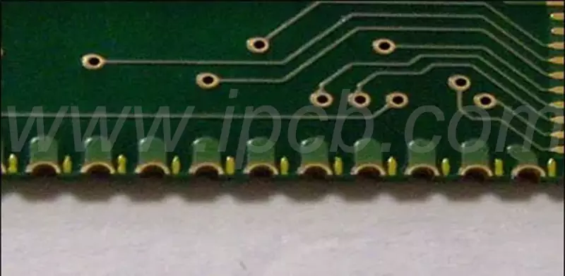
Here are a few key points to keep in mind:
A copper strip is required on each side to ensure an effective plating connection.
During the plating process, the board needs to be held in place so that the edges cannot be fully plated.
If rounded edge plating is required, it should be clearly labelled in the mechanical layer.
The only suitable surface treatment for rounded edge plating is selective electroless nickel gold.
The manufacturing process for pcb edge plating presents a number of challenges such as precise machining, edge pre-treatment and burr prevention, all of which have a direct impact on the adhesion and electrical properties of the plated layer. To ensure the successful implementation of plating, manufacturers need to adopt the following controls:
Accurate Thickness Management: Ensure that the plating layer meets the established minimum thickness criteria.
Electrical Continuity Verification: Ensure that the current path is unobstructed from the inner layer to the edge contact point.
Plating Coverage Uniformity Audit: Avoid weak areas or voids to ensure robust mechanical and electrical performance.
Over-plating prevention: Regulate plating thickness to prevent connector fitment from being compromised.
Trace geometry verification: Ensure compliance with design specifications to avoid adverse effects on electrical performance.
Edge plating plays a key role in enhancing the current loading capability of PCBs, providing reliable edge connections, protecting edges from damage, facilitating edge soldering, and improving overall manufacturing quality. When planning for edge plating, designers need to work closely with the manufacturer to clearly identify edge plating needs and surface finish requirements, as well as keep a reasonable distance between the internal power layer and the edges to ensure a smooth manufacturing process. Through rigorous process control, edge plating can meet the needs of a wide range of industry applications, especially where the reliability of the on-board connections is of paramount importance.
As an important process in modern electronics manufacturing, PCB edge plating not only improves the board’s electromagnetic compatibility, current loading capacity and durability, but also provides designers with more flexible and reliable edge connections. From wrap-around edge plating to copper edge treatments, through-hole plating on board edges and rounded edge plating processes, each type of plating carries specific application and performance requirements.
To ensure the successful implementation and high quality output of pcb edge plating, manufacturers must pay close attention to every detail of the plating process, from the availability of specialised equipment and expertise,to pre-treatment and preparation,to enhancement of plating adhesion, precise soldering control, and the prevention of burr generation – every step is critical.At the same time,designers should also maintain close communication and collaboration with manufacturers to develop clear design rules and plating requirements to ensure that the final product meets performance and reliability expectations.
As electronics technology continues to evolve and industry applications become more diverse, PCB edge plating technology will continue to play an important role in enhancing the performance and reliability of electronic products. In the future, we look forward to seeing more innovative plating technologies and solutions that will bring more efficient, reliable and sustainable development to the electronics manufacturing industry.
