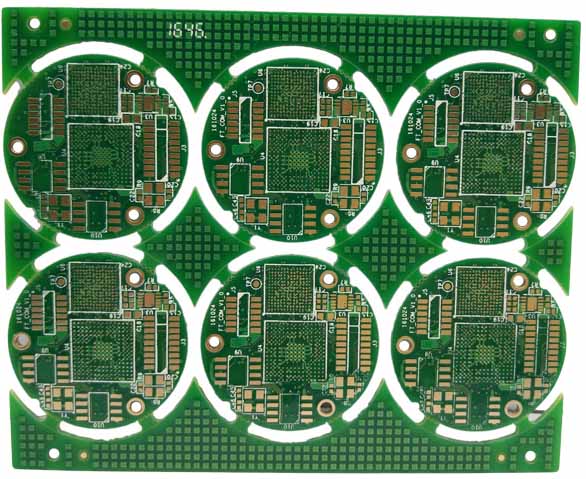
Common pcb panel sizes (which can be considered industry standards) include: 24” x 18”, 12” x 18”, and 24” x 9”. Note that these panels have 0.5” margins on all sides and 0.1” space between the individual boards that make them up. It is also worth noting that the 24 x 18” panel is the most common and many companies will use it to manufacture different PCB sizes.
PCB board sizes vary depending on the application and design requirements and can come in a wide variety of sizes.
Custom Sizes:
In addition to standard sizes, PCBs can be customized to meet the needs of specific applications. These can be rectangular, square, round, or other shaped boards.
Small Sizes:
Some applications require small PCBs, such as chip-scale PCBs used in miniature electronic devices, which may only be a few millimeters in size.
Large Sizes:
Some special applications, such as high-powered power supplies, large electronic devices, etc., may require large PCBs that can be several feet or even larger in size.
Elongated Sizes:
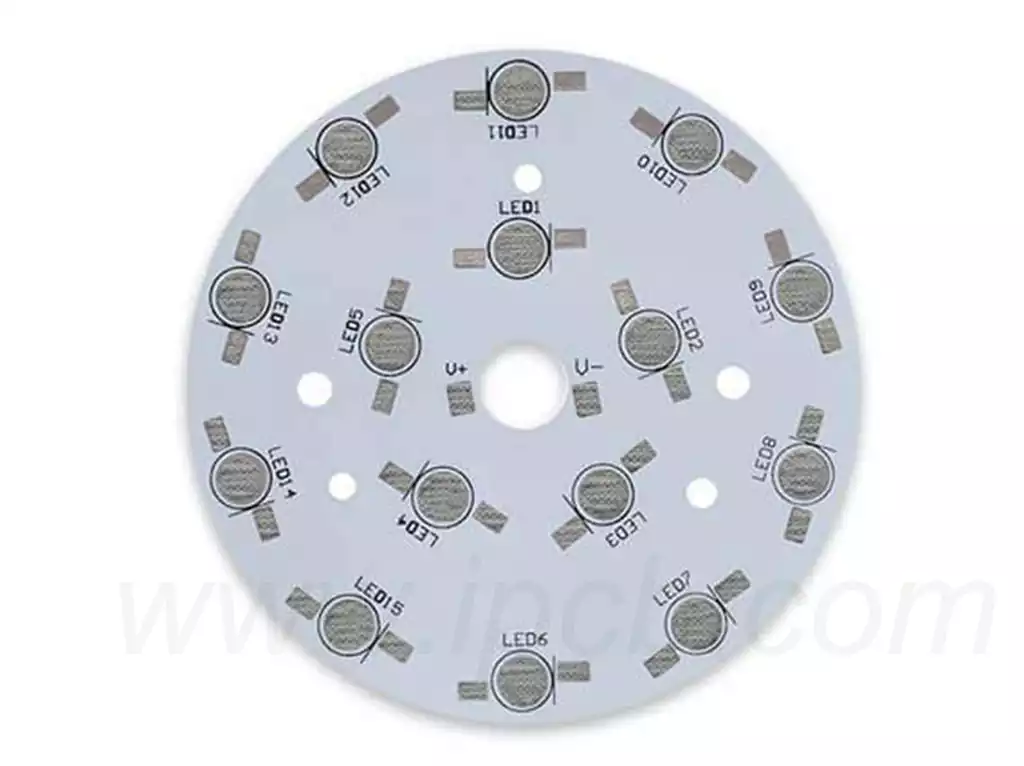
In some specific applications, elongated PCBs may be required, such as LED lighting strips.
Flexible PCB size:
Flexible PCB can be designed into various shapes and sizes according to bending or folding requirements.
Rigid-flexible PCB size:
Rigid-flexible PCB combines the characteristics of rigid board and flexible board, and can adapt to applications with special shapes or space restrictions.
Basic requirements for FR-4 copper-clad PCB size
- Product size
The size of the product is expressed by multiplying the length by the width. There are two ways of expressing the unit: imperial and metric (see Table 25).
(1) Imperial: Usually expressed in inches (read inches), the imperial specifications are usually 36 inches × 48 inches; 40 inches × 48 inches; 42 inches × 48 inches; because users want to increase the material yield, the requirements for product size are gradually increased, and there are 36.5 inches × 48.5 inches; 37 inches × 49 inches; 42.5 inches × 48.5 inches; 41 inches × 49 inches; 43 inches × 49 inches and other specifications.
(2) Metric: usually expressed in mm. Since 1 inch = 25.4 mm, the metric specifications are: 914×1220 mm (36 inches × 48 inches = 914×1220 mm); 927×1232 mm (36.5 inches × 48.5 inches); 940×1245 mm (37 inches × 49 inches); 1016×1219 mm (40 inches × 48 inches); 1029×1232 mm (40.5 inches × 48.5 inches); 1067×1219 mm (42 inches × 48 inches); 1080×1232 mm (42.5 inches × 48.5 inches); 1042×1245 mm (41 inches × 49 inches); 1093×1245 mm (43 inches × 49 inches). - Straightness
Straightness is the degree of perpendicularity between the long side and the wide side of the product. In order to improve the material yield, the product is required to have a higher straightness.
Since it is troublesome to use angle detection to measure the straightness, and since the deviation of the two diagonals of the product is in correspondence with the straightness of the product, the straightness of the product can be checked by measuring the two diagonals of the product. In actual production, most manufacturers also use the method of measuring the deviation of the two diagonals of the product to reflect the straightness of the product, and usually require that the deviation of the two diagonals of the product does not exceed 2 mm.
Almost all devices have printed circuit boards. However, not every device has the same size. For example, compared with TVs, smartphones require very small PCBs. Compared with heavy machinery, TVs require smaller PCBs. Therefore, these sizes play a vital role in the circuit. Designers must design the PCB size according to the size of the device
Calculation of PCB panel size
The size usually depends on the components in the circuit. How dense it is and how many through-holes or connectors there are. Calculate the pcb panel size according to the instructions given.
Open the layout design in the software. The layout will show an outline containing the components. Take the components according to the circuit diagram.
After placing the components, increase or decrease the size of the PCB outline. Leave at least half an inch area around the edge of the circuit
Measure the size. Multiply this size with the vertical and horizontal lines of the box, and you get the size of the board
Factors for choosing the right size
There are many factors to consider when choosing the size, keep in mind the factors mentioned below:
Weight: Check the weight of the device for which the circuit is being made. Do not use thinner boards unless necessary. Because thinner boards break easily
Flexibility: Thick boards are heavier and less flexible. Thin boards are more flexible. However, they can get broken easily. Use the circuit board according to the required circuit. For example, a smartwatch may require a flexible circuit, while a computer motherboard requires a thick board.
Basic rules for PCB wiring
- It is forbidden to draw wiring in the area ≤1mm from the edge of the PCB board and within 1mm around the mounting hole.
- The power line should be as wide as possible, not less than 18mil; the signal line width should not be less than 12mil; the CPU input and output lines should not be less than 10mil (or 8mil); the line spacing should not be less than 10mil.
- Normal vias should not be less than 30mil.
- Note that the power line and the ground line should be as radial as possible, and the signal line should not have loop routing.
- Ground loop rules:
- Crosstalk control
- Routing direction control rules:
- Routing open loop inspection rules:
- Impedance matching inspection rules:
- Routing closed loop inspection rules:
- Routing branch length control rules:
Try to control the length of the branch, the general requirement is Tdelay<=Trise/20.
- Routing resonance rules:
Mainly for high-frequency signal design, that is, the wiring length must not be an integer multiple of its wavelength to avoid resonance.
- Routing length control rules:
- Chamfer rules:
Avoid sharp angles and right angles in PCB design, which will cause unnecessary radiation and poor process performance.
- Device layout partition/layering rules
For mixed circuits, there is also a way to distribute analog and digital circuits on both sides of the printed circuit board, use different layers for wiring, and isolate them in the middle with ground layers.
- Isolated copper area control rules:
The emergence of isolated copper areas will bring some unpredictable problems. Therefore, connecting isolated copper areas with other signals will help improve signal quality. Usually, isolated copper areas are grounded or deleted. In actual production, PCB manufacturers add some copper foil to the vacant parts of some boards, mainly to facilitate printed circuit board processing, and also to prevent printed circuit board warping. - Integrity rules for power and ground layers:
For areas with dense vias, care should be taken to avoid holes connecting to each other in the hollowed-out areas of the power and ground layers, forming a division of the plane layer, thereby destroying the integrity of the plane layer, and then causing the signal line to increase the loop area in the ground layer. - Overlapping power and ground layer planning:
Different power layers should avoid overlapping in space. The main purpose is to reduce the interference between different power supplies, especially between power supplies with large voltage differences. The overlap of power planes must be avoided. If it is difficult to avoid, consider using a bottom layer in the middle. The power bus that supplies power between different signal layers follows this rule, that is, try to avoid overlap. - 3W rule
In order to reduce crosstalk between lines, the wire spacing should be large enough. When the center spacing of the wires is not less than 3 times the line width, 70% of the electric fields can be kept from crosstalking each other. If 98% of the electric fields do not interfere with each other, a 10W spacing can be used. When the wiring density is low, the spacing between signal lines can be appropriately increased. Signal lines with large differences in high and low levels should be as short as possible and the spacing should be increased. - Width of printed conductors: The conductor width should be suitable to meet the electrical performance requirements and be easy to produce. Its minimum value is determined by the current it bears, but the minimum should not be less than 0.2mm. In high-density, high-precision printed circuits, the conductor width and spacing can generally be 0.3mm; the conductor width should also consider its temperature rise under high current conditions. Single-panel experiments show that when the copper foil thickness is 50μm, the conductor width is 1~1.5mm, and the current is 2A, the temperature rise is very small. Therefore, generally, a conductor with a width of 1~1.5mm may meet the design requirements without causing temperature rise; the common ground wire of the printed conductor It should be as thick as possible. If possible, use lines larger than 2 to 3 mm. This is especially important in circuits with microprocessors, because when the ground line is too thin, the noise tolerance will be degraded due to the change of the current flowing through, the change of the ground potential, and the instability of the level of the microprocessor timing signal; the 10-10 and 12-12 principles can be applied to the routing between the IC pins of the DIP package, that is, when two wires pass between the two pins, the pad diameter can be set to 50mil, the line width and line spacing are both 10mil, and when only one wire passes between the two pins, the pad diameter can be set to 64mil, the line width and line spacing are both 12mil.
- Shielding and grounding of printed conductors: The common ground wire of the printed conductor should be arranged at the edge of the printed circuit board as much as possible. On the printed circuit board, as much copper foil as possible should be retained as the ground wire. The shielding effect obtained in this way is better than that of a long ground wire, the transmission line characteristics and shielding effect will be improved, and the distributed capacitance will also be reduced. The common ground wire of the printed conductor is preferably formed into a loop or mesh. This is because when there are many integrated circuits on the same board, especially components with high power consumption, the ground potential difference is generated due to the limitation of the pattern, which causes the noise tolerance to decrease. When it is made into a loop, the ground potential difference decreases. In addition, the ground and power patterns should be parallel to the flow direction of the data as much as possible. This is the secret to enhancing the ability to suppress noise; multi-layer printed circuit boards can use several layers as shielding layers, and the power layer and ground layer can be regarded as shielding layers. Generally, the ground layer and power layer are designed in the inner layer of the multi-layer printed circuit board, and the signal line is designed in the inner and outer layers.
This is part of the content about pcb panel size and pcb layout. If you need it, please do not hesitate to contact us.
