A pcb microscope is a microscope specifically designed to observe printed circuit boards (pcbs). In the modern electronics industry, pcb microscopes play a key role in helping engineers and technicians inspect and analyze tiny and delicate circuit structures in electronic devices.
As a pcb manufacturer, efficient and reliable pcb quality control (QC), rework, failure analysis, and research and development (R&D) inspections are essential to achieve cost-effective production and competitive electronic products. The performance of a pcb is significantly affected by soldering, vias, diodes, IC chips, and other components. All of these must be inspected. To demonstrate compliance with specified specifications, imaging solutions that enable reliable and accurate documentation are often required. pcb microscopes help us meet their quality control, failure analysis, and R&D needs.
What is pcb inspection and why is it important?
pcb inspection is essential for quality control to ensure optimal performance of electronic components and economical, reliable pcb production. During manufacturing and production, visual inspection of circuit boards is performed to identify potential damage defects in soldering, leads, component contacts, particles, and other contaminants.
What types of microscopes are used for pcb inspection?
Digital pcb microscopes are ideal for inspection. When looking for defects or rework: These microscopes easily handle PCS under the objective lens, can directly use different types of lighting to better reveal details, and can quickly change from an overview to a zoomed-in area of interest. Stereo microscopes with FusionOptics provide a three-dimensional perception of the pcb, with higher resolution and greater depth of field.
What is the best magnification for pcb inspection?
The practical magnification range for pcb inspection using a stereo or pcb microscope is 5 to 30x (including objective, zoom and eyepiece). This range allows both a general overview of the pcb area at lower magnifications (approximately 5x) and visualization of details at higher magnifications (approximately 25-30x).
Efficiently screen pcbs and document results
pcb inspection should be fast and reliable. A pcb microscope solution should allow the user to:
Get an overview of the sample and easily zoom in on areas of interest
Reveal more details with versatile lighting
Easily handle or move samples under the objective due to the large working distance
Record results in less time
Stay comfortable and avoid fatigue even during all-day inspections.
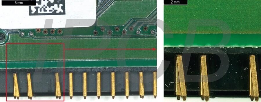
pcb microscope
(Left) Bent connector pins at lower magnification. Right) Zoomed in red boxed area for more details
Fast 3D pcb inspection
If 3D perspective is important for pcb processing and rework, a stereo microscope is needed. Frequent microscope adjustments, such as refocusing and changing magnification to improve resolution and depth of field, can slow down inspections. These adjustments can be minimized with FusionOptics technology. When looking through the eyepieces, the technology allows you to observe 3D stereo images with high resolution and large depth of field.
pcb cleanliness analysis
pcb cleanliness is important because small conductive particles can significantly increase the risk of failure. If these particles are present on the pcb during the manufacturing process, they can easily bridge the small gaps between contacts and leads, causing short circuits.
Therefore, fast and reliable cleanliness analysis of pcbs is required to minimize or eliminate contamination and ensure pcb performance. This analysis involves accurate determination of particle size and material in accordance with standards and guidelines such as ZVEI. Cleanliness analysis can be performed using optical microscopy alone or in combination with laser induced decomposition spectroscopy (LIBS). Chemical analysis using LIBS helps to accurately determine the likelihood of particles causing short circuits and efficiently find the source of contamination.
pcb cross-sectional analysis
In order to observe the internal structure of the pcb to identify defects, cross-sectional cutting is required because the material is usually opaque. Cross-sectional analysis is a useful technique for pcb quality control. It can also be used in failure analysis and R&D. The analysis is performed by cutting the pcb and then grinding and polishing the cross section to obtain a smooth surface. Cross-sectional analysis can be performed by high-resolution optical or electron microscopy and spectroscopy. Its purpose is to reveal the internal structure and composition of the pcb layer and its components, confirming the presence of coatings, through-holes, etc.
Plating of pcb components
Electroplating is an electrochemical process used to deposit a protective metal layer, such as copper or tin, onto pcb connectors or components. Defects and contamination during the plating process can lead to poor plating quality or even pcb failure. Optical microscopy allows for quick and reliable visual inspection of plated components for defects. If root cause analysis of defects or contamination is required, a combination of optical microscopy and laser induced decomposition spectroscopy (LIBS) is recommended for simultaneous visual and chemical analysis.
How can digital microscopy assist in achieving a reliable analysis process and improving work efficiency?
Digital pcb microscopes have a variety of powerful features that are not only easy to use, but also improve the efficiency of QC, FA and R&D work:
The software for microscope operation and data analysis is very intuitive;
Supports efficient and simple changes in magnification across the entire range (12× to 2,350×);
Encodes important parameters (automatically tracked and stored), such as stage, optics, lighting and camera settings, for quick access at any time;
Lens tilt and sample rotation are convenient and fast;
Integrated LED (light-emitting diode) ring light and coaxial lighting can present a variety of contrasts;
High-performance digital camera can quickly capture real-time images with a resolution of 10 MP;
Software enables/supports capture modes such as XY and XYZ stitching, high dynamic range (HDR) images, etc.
- Technical features
1.1 High magnification
pcb microscopes usually have high magnification, which can clearly observe the tiny details of the pcb surface, helping to find potential defects or problems.
1.2 Non-contact observation
The use of non-contact observation technology prevents damage to the pcb during observation and ensures the integrity of the circuit board.
- Application fields
2.1 Manufacturing and assembly
During the manufacturing and assembly of pcbs, pcb microscopes are widely used to check solder joints, trace circuit lines, and verify assembly quality.
2.2 Electronic repair
In the repair of electronic equipment, pcb microscopes help technicians locate and repair faults on circuit boards.
- Usage tips
3.1 Cleaning and maintenance
Keep the optical components of the pcb microscope clean and perform regular maintenance to ensure image quality during observation.
3.2 Appropriate lighting selection
Choose appropriate lighting methods according to the characteristics of different pcbs to highlight key details.
- Future development trends
4.1 Digitalization and intelligence
In the future, pcb microscopes may tend to be digitalized and intelligent, providing more data support through image processing and analysis technology.
4.2 High-resolution technology
With the advancement of optical technology, pcb microscopes are expected to provide higher resolution, and fine structures will be more clearly visible.
- Successful Cases
5.1 Electronic Manufacturing
In the electronic manufacturing industry, pcb microscopes help improve production efficiency and ensure that the quality of circuit boards meets standards.
5.2 Electronic Repair Services
In electronic repair services, pcb microscopes are used to locate and repair circuit faults in mobile phones, computers and other devices.
pcb Appearance Inspection
Appearance inspection is to analyze the appearance characteristics of the pcb to determine whether it meets the design requirements and production standards. Common appearance inspection methods include visual inspection, optical pcb microscope inspection and digital image processing technology.
Visual inspection is the simplest method. It observes the pcb with human eyes to determine whether there are defects such as welding problems and short circuits.
Optical microscope inspection can magnify details and help detect minor welding problems and friction marks.
Digital image processing technology combined with image processing algorithms can automatically detect various defects on pcbs and improve inspection efficiency and accuracy.
pcb Internal Quality Inspection
Internal quality inspection is to inspect the internal wires and inner layers of the pcb to ensure the quality of circuit connections. Common internal quality inspection methods include perspective inspection, X-ray inspection and probe testing.
Perspective testing is to observe the perspective view of the pcb to determine whether the wire is complete and whether there are any problems such as breakage.
X-ray testing can penetrate the pcb to detect the internal welding quality and line connection.
Probe testing is to use special test instruments to test the contact points of the pcb wires to determine their current transmission capacity and signal integrity.
The combined application of these internal quality testing methods can fully guarantee the reliability and stability of the internal line connection of the pcb.
Common problems and challenges
Detection and treatment of foreign matter in pcbs: Foreign matter such as dust and water droplets may affect the normal operation of the pcb, so it is necessary to detect and handle them in time during the detection process.
Detection and evaluation of pcb materials: The material quality of pcbs directly affects their carrying capacity and conductive properties, so it is necessary to ensure that the materials used meet the relevant standards and requirements.
pcb structure and process problems: such as whether the copper foil layering is uniform and whether the direction of the wire is reasonable.
pcb appearance and internal quality inspection are important links to ensure the high quality of electronic products. Through the comprehensive application of appearance inspection and internal quality inspection, pcb problems can be discovered and solved in time to ensure the reliability and stability of circuit connections.
In practical applications, we also need to combine specific detection needs and equipment conditions to select appropriate detection methods and process flows. Only by continuously improving and perfecting the appearance and internal quality detection technology of pcbs can we meet the ever-increasing quality requirements of electronic products.
Overall, as an indispensable tool in the electronics industry, pcb microscopes reveal the subtle beauty behind tiny circuits for us. Through its high magnification and precision observation technology, engineers can gain a deeper understanding of the internal structure of electronic equipment, improve production efficiency and product quality. In the future, with the continuous development of science and technology, pcb microscopes will usher in greater breakthroughs in digitalization, intelligence and high resolution, bringing more innovation and convenience to the electronics industry.
