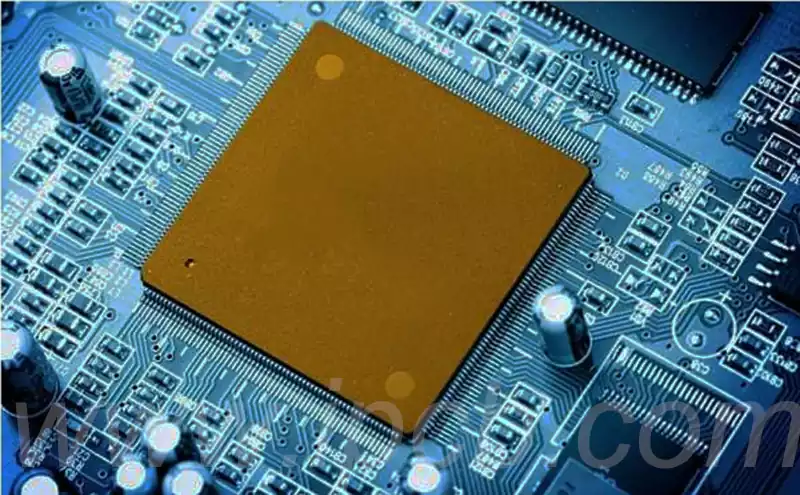
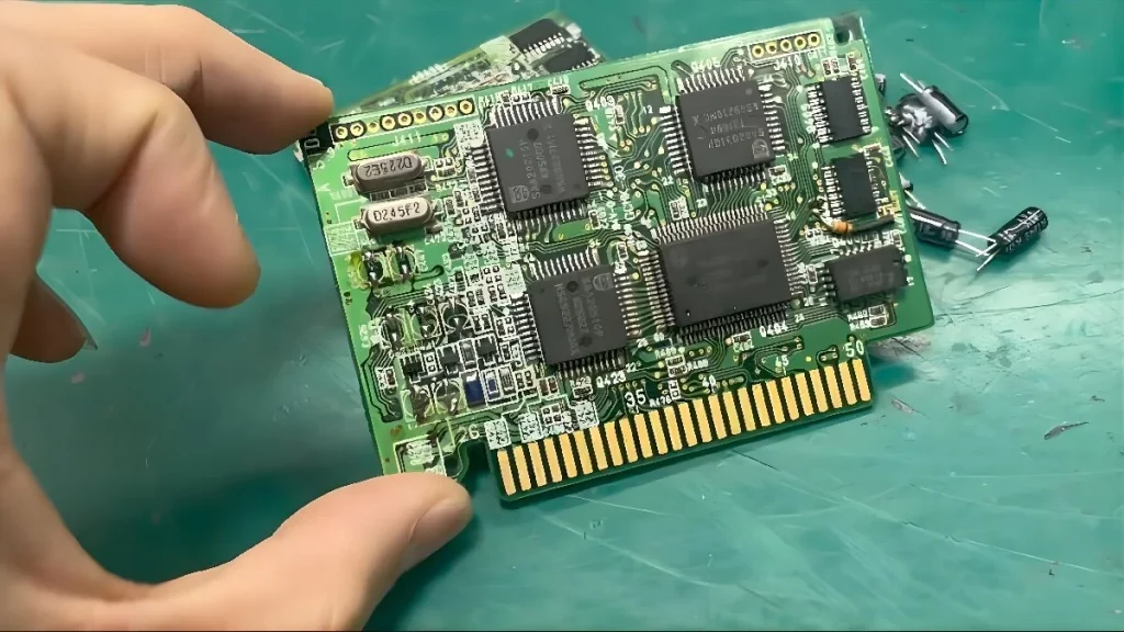
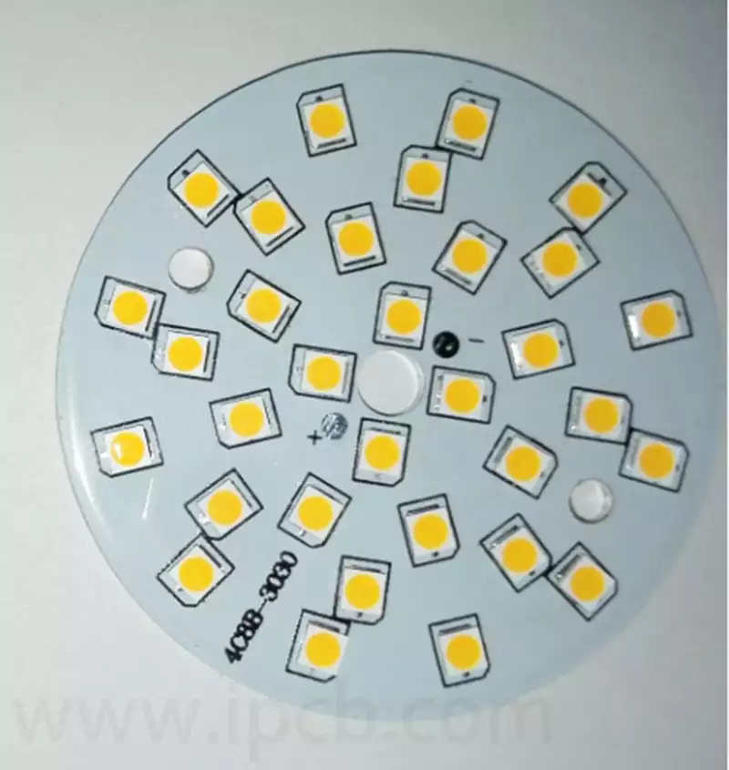
The x-ray machine for pcb is a non-destructive inspection device for printed circuit boards using the X-ray transmission principle. With the help of X-ray imaging, it is able to accurately visualise the internal structure of the PCB as well as the subtleties of the solder joints, such as holes in the solder joints, defective soldering, short circuits and broken circuits. Without disassembling or damaging the PCB, this inspection technology quickly and accurately identifies defects in the production process, thereby improving product quality and reliability.
The principle of x-ray machine for pcb is not complicated.When a cathode electron collides with a metal target, it suddenly decelerates, releasing a large amount of energy.
This energy is radiated outwards in the form of X-RAY. It is worth noting that the energy of x-ray machine for pcb is closely related to the density of the substance. Substances of different densities absorb X-RAY to different degrees, so we can distinguish between substances of different densities by their X-RAY penetration ability. When X-RAY irradiates an object, most of the energy will penetrate the object and only a small portion will be absorbed. Using this property, we can analyse the internal structure of an object. If the thickness or shape of an object changes, the X-RAY absorbed image will produce corresponding black and white changes. By magnifying these images, we can clearly see the defects inside the object.X-RAY has a very short wavelength and has a high penetrating power. This makes it ideal for flaw detection on thin-walled workpieces, which are very sensitive to volumetric defects. At the same time, x-ray machine for pcb provides realistic defect images and accurate dimensional measurements. The basic process is as follows :
X-ray generation: The X-ray source is responsible for generating a beam of high-energy X-rays, which is then directed onto the PCB to be tested.
X-ray transmission process: As the X-rays pass through the PCB, the intensity of the transmitted X-rays varies due to differences in X-ray absorption between the different materials and structures within the PCB.
Image Capture: X-rays transmitted through the PCB arrive at a detector (e.g. flat panel detector or CCD camera), which further converts these X-ray signals into visible or electrical signals to form an image.
Image analysis: The image captured by the detector is analysed and processed in depth with the aid of image processing software to produce a high resolution X-ray image. This image can be scrutinised by the inspector to assess the quality of the PCB.
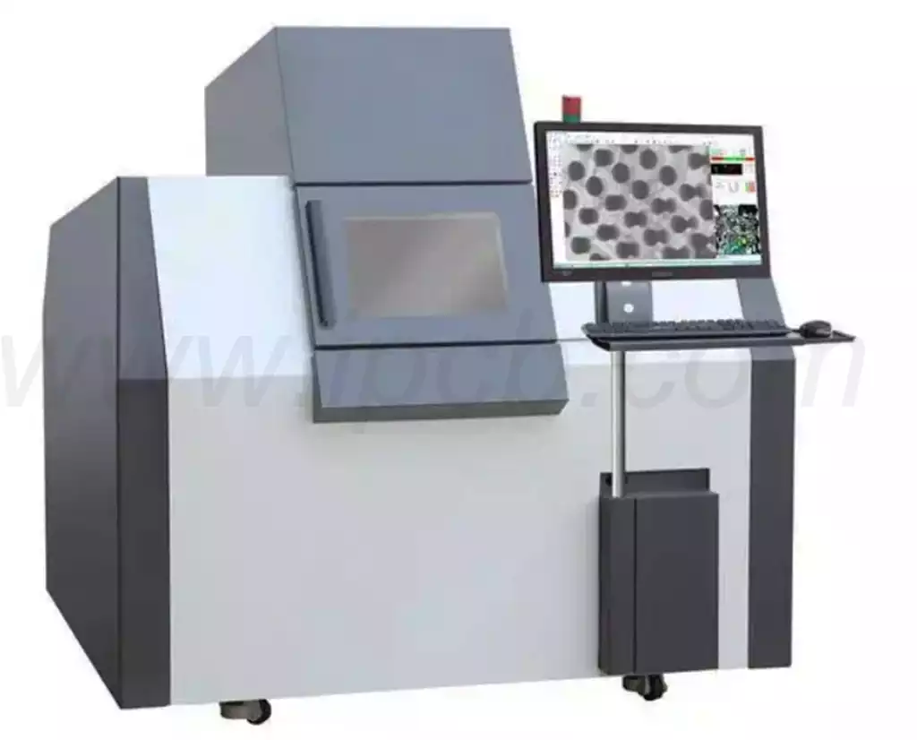
X-ray machine for pcb in smt applications
In the field of SMT (Surface Mount Technology) processing, X-ray inspection devices play a pivotal role. Compared to traditional ICT (in-circuit tester) inspection methods, X-ray in the BGA (ball grid array package) solder joints in the internal structure of the inspection of the accuracy of more than 15 per cent, and the efficiency of the increase of up to 50 per cent. X-RAY inspection device is extremely wide range of applications, which is not only able to accurately identify the BGA internal soldering defects such as empty soldering, false soldering, etc., but also able to microelectronic components, seals, cables, fixtures and even plastic parts. This is why X-RAY inspection devices have become an indispensable tool in the SMT field.
Non-destructive perspective: x-ray machine for pcb provides the SMT production line with a non-destructive view of the inside.With this technology, engineers are able to clearly observe the construction details inside the printed circuit board, including areas that are difficult to reach with the naked eye, such as the soldering points on the underside of BGAs, CSPs (Chip-Size Packages), and so on.
Enhanced Manufacturing Quality: With X-RAY inspection, production lines are able to quickly catch defects in the soldering process, such as false soldering, solder ball shift, bridging, etc., which significantly enhances product stability and manufacturing quality.
Cost control: Timely detection and correction of defects in the production process effectively avoids the generation of a large number of defective products, which in turn reduces the cost of rework and waste and saves the company a lot of money.
Comply with the trend of miniaturisation and high-density assembly: With the continuous reduction of component size and the trend of high-density assembly of circuit boards, the traditional means of optical inspection are no longer adequate. X-RAY inspection is the ideal choice for miniaturisation and high-density assembly due to its excellent resolution and in-depth detection capability.
Strengthen market competitiveness: Manufacturers with advanced X-RAY inspection capabilities tend to win the trust of more customers, giving them an edge in a competitive marketplace.
Meet stringent standards: For industries such as aerospace, medical and military, where product reliability is critical, X-RAY inspection is an indispensable means of ensuring compliance with quality standards and safety requirements.
With its non-destructive, high-precision and high-efficiency features, x-ray machine for pcb shows great potential and value in the SMT field. It can not only help manufacturers find and correct defects in the production process in a timely manner, improve product quality and reliability, but also effectively control costs and enhance market competitiveness. With the miniaturisation of components and the continuous development of the trend of high-density assembly of circuit boards, the PCB X-ray inspection machine will play a more important role and become an indispensable key tool to ensure product quality and safety.
