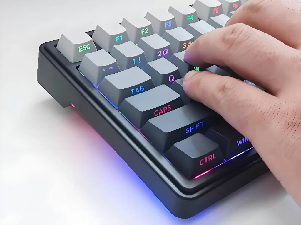
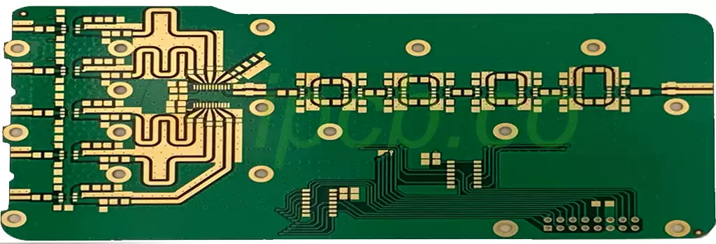
In the mechanical keyboard DIY circle, custom keyboards are not only a hobby, but also a way to show creativity and personalization. What Tool to Cut Keyboard PCB? In order to achieve the ideal keyboard layout and size, cutting the keyboard PCB has become one of the skills that many players must master. In addition to the tools and techniques mentioned above, here we continue to explore the process of cutting PCBs, the detailed use of tools, and more relevant experience to help you master the cutting technology more comprehensively.

Preliminary preparation for PCB cutting
Before cutting, preparation is essential. The following steps can help you complete the cutting task more efficiently and safely.
- Determine the cutting needs
First, you must clarify your cutting goals: is it to reduce the size of the keyboard, or to adjust the layout to be compatible with a special shell? Different needs will determine the method and scope of cutting. For example, if you want to reduce the size, you may need to cut off the edge of the PCB, while adjusting the layout may involve cutting off part of the function key area. - Plan the cutting line
Use CAD tools or draw the cutting drawings by hand. Mark the cutting line with a marker on the PCB surface, while making sure to avoid key circuit areas, such as key signal lines, power rails, and ground lines. If there are no relevant design files or you are not sure about the feasibility of cutting, you can consult experienced players or check the official PCB schematics. - Tool preparation and inspection
Different cutting tools are suitable for different PCB types and cutting needs. According to the tools mentioned above, choose the appropriate equipment and make sure they are in good condition. Check whether the cutting disc is sharp, whether the laser machine is calibrated, and whether the saw blade is firm to avoid affecting the cutting quality or causing safety hazards. - Protective measures
Fine debris or smoke may be generated during the cutting process. Wearing goggles and masks is a basic safety guarantee. In addition, protective gloves should be worn to prevent your hands from being scratched by sharp PCB edges.
Detailed operation skills of cutting tools
Here are some additional tips for commonly used tools to further improve cutting efficiency and effect:
In-depth application of electric cutting machines
Electric cutting machines are suitable for tasks that need to be completed quickly, but pay attention to the following points when using them:
Speed adjustment: Adjust the speed of the cutting machine according to the thickness and hardness of the PCB material. Too high a speed may cause the cutting surface to overheat, thereby damaging the circuit board.
Cooling measures: During the cutting process, use coolant or fan to reduce the temperature of the cutting area to prevent the copper foil from peeling off due to high temperature.
Cutting posture: Fix the cutting machine with both hands and keep it perpendicular to the PCB surface to obtain a straight cutting line.
Detailed debugging of laser cutting machine
Although the laser cutting machine is accurate, it also needs some parameter debugging according to the characteristics of the PCB:
Power control: Too high power may cause excessive ablation of the PCB, and too low power will not be able to cut through. It is recommended to start from low power and gradually increase to a suitable level.
Focal length adjustment: Make sure that the laser focus is on the cutting area, so that a narrower cutting line can be obtained.
Auxiliary gas: Some laser cutting machines support the use of auxiliary gas (such as compressed air), which can improve cutting efficiency and reduce thermal damage.
Flexible application of manual tools
For players who do not need high-frequency cutting, manual tools are still an important choice:
Saw blade selection: Choose a fine-toothed saw blade designed for metal or PCB to reduce tearing during cutting.
Steady hands and careful heart: When operating manually, pay attention to keeping the cutting line stable and try to avoid repeated cutting back and forth, which will affect the flatness of the edge.
Cleaning and repairing after cutting
After cutting, cleaning and repairing the PCB is an important part of ensuring its normal function.
- Edge grinding
The edges of the cut PCB are usually sharp, which is not only easy to scratch, but also may affect the installation accuracy. Use the following tools for grinding:
File: Suitable for fine edge processing, you can choose flat file or round file according to your needs.
Sandpaper: Starting from coarse sandpaper (such as 400 mesh) to fine sandpaper (such as 1000 mesh) can make the edge smoother.
Electric grinder: For large-area cutting, you can consider using a small electric grinder.
- Circuit test
The cut PCB needs to be fully electrically tested to ensure that the conductivity of all circuits is not affected. The following methods can be used:
Multimeter test: Check whether the signal line and power line are connected normally.
Power-on test: On the premise of confirming safety, power on the PCB to check whether there are abnormal conditions such as short circuit and overload.
- Soldering Remediation
If some pads or traces are damaged during cutting, they can be repaired in the following ways:
Jumper welding: Use wires to reconnect the disconnected signals.
Pad repair sheet: There are special PCB pad repair sheets on the market, which can be pasted on the damaged area for repair.
Soldering supplement: Use solder to fill the pads or conductive areas damaged during cutting.
Cutting solutions for special situations
In actual operation, some special situations may be encountered. The following are the corresponding solutions:
Multi-layer PCB cutting
For multi-layer PCBs, the cutting difficulty increases significantly because the internal copper layer and insulation layer need to be processed at the same time. It is recommended to use a laser cutting machine or a high-precision electric cutting machine to complete it, and check the circuit layer by layer after cutting to see if it is complete.
Curved cutting
Sometimes, in order to adapt to a specific shell, it may be necessary to make curved or special-shaped cuts on the PCB. At this time, a small hand saw can be used with sandpaper for gradual trimming, or it can be done directly with a laser cutting machine.
PCB with gold fingers
The gold finger area (connector part) is a more sensitive area in the PCB and should be avoided as much as possible during cutting. If the area must be cut, ensure that the cut is smooth and use special tools to polish it to avoid affecting the contact performance.
Issues to pay attention to during cutting
Cutting PCBs requires not only technical support, but also safety and quality control:
Avoid overcutting: The cutting range should be as small as possible to prevent accidental damage to key circuits.
Keep the workbench clean: The debris generated during the cutting process may be conductive and easily cause short circuit problems, so it should be cleaned up in time.
Multiple checks: After cutting, the circuit function should be repeatedly confirmed to be complete to avoid rework waste.
Extended knowledge of post-processing of PCB cutting
Cutting PCBs is only a staged task, and post-processing is also crucial.
Edge protection
Even if the cutting edge has been polished flat, it may wear or peel off during long-term use. To solve this problem, some additional protection measures can be used, such as:
Applying a layer of PCB protective paint on the cutting edge can prevent the copper layer from oxidizing and getting wet.
Install a protective cover: Some high-end keyboard players use a customized plastic frame to completely cover the cutting edge to enhance the overall aesthetics and durability of the keyboard.
Stability test after cutting
The cutting of PCB may have an impact on mechanical strength, especially if the cutting area is close to the fixing holes or load points of the PCB. Therefore, the stability after cutting can be tested in the following ways:
Vibration test: Lightly tap the PCB to check for cracks or signs of looseness.
Bending test: Apply moderate bending force to confirm the strength of the cutting area.
Functional verification
After completing all physical processing, the last step is to fully test the function of the PCB. You can build a simple test platform to simulate the actual use environment of the keyboard to confirm that each key can respond normally.
Future development and technological progress
PCB cutting technology is constantly improving with the advancement of tools. For example:
Intelligent cutting equipment: Cutting machines with AI recognition functions can automatically detect key circuit areas to avoid cutting errors.
Environmentally friendly cutting technology: In order to reduce electronic waste, many manufacturers are developing more environmentally friendly cutting methods, such as cutting discs made of renewable materials or equipment that reduces dust emissions.
Automated assembly line: In the future, customized PCBs may be highly integrated with cutting technology. Players only need to define their requirements in the software, and the factory can directly output customized cut PCBs.
Summary
Cutting keyboard PCB is a challenging and creative skill in mechanical keyboard DIY. In selecting tools, planning cutting routes and subsequent processing, players need to fully consider their own needs and operating capabilities. By making rational use of tools such as electric cutters, laser cutters, hand saws, and combining circuit testing and repair techniques, personalized keyboard customization can be easily achieved. Whether you are a novice or an experienced player, I hope this article can provide practical help and inspiration for your DIY journey!


