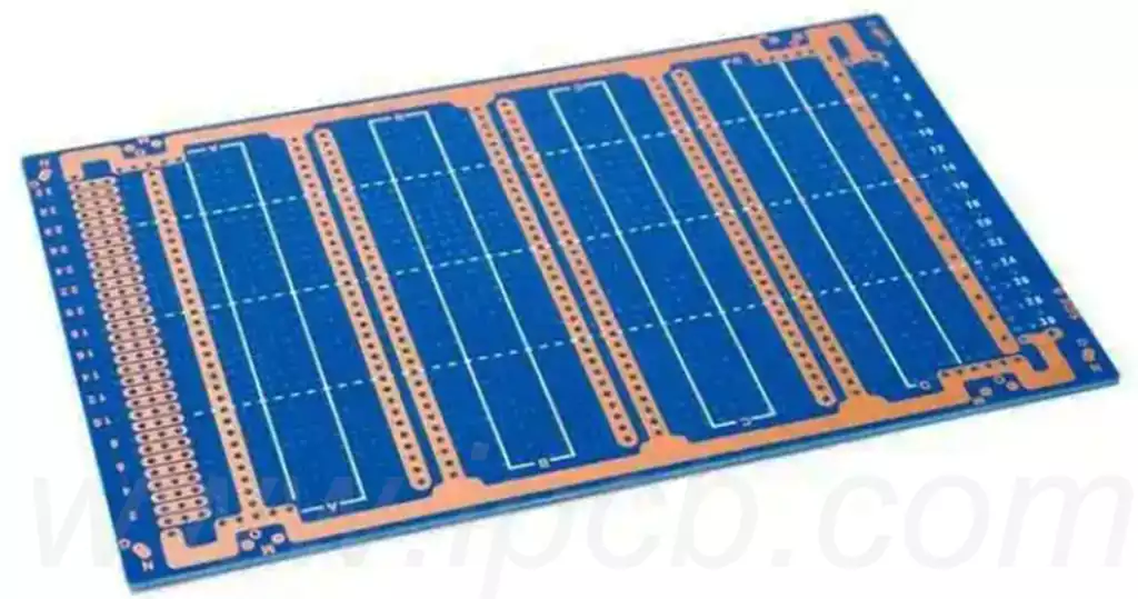
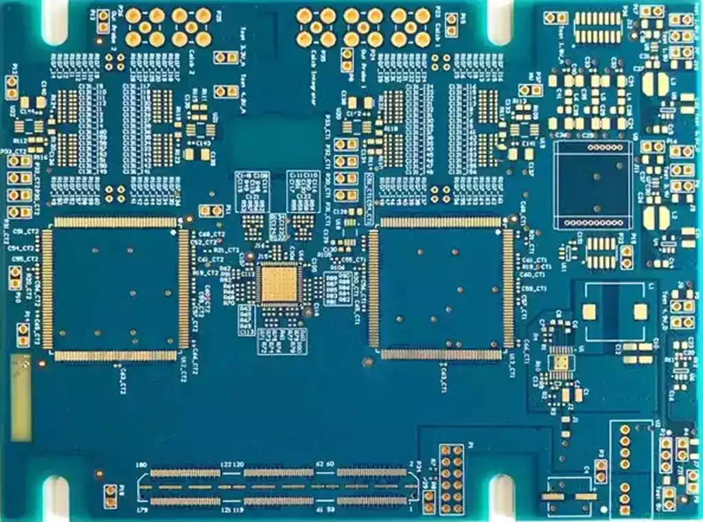
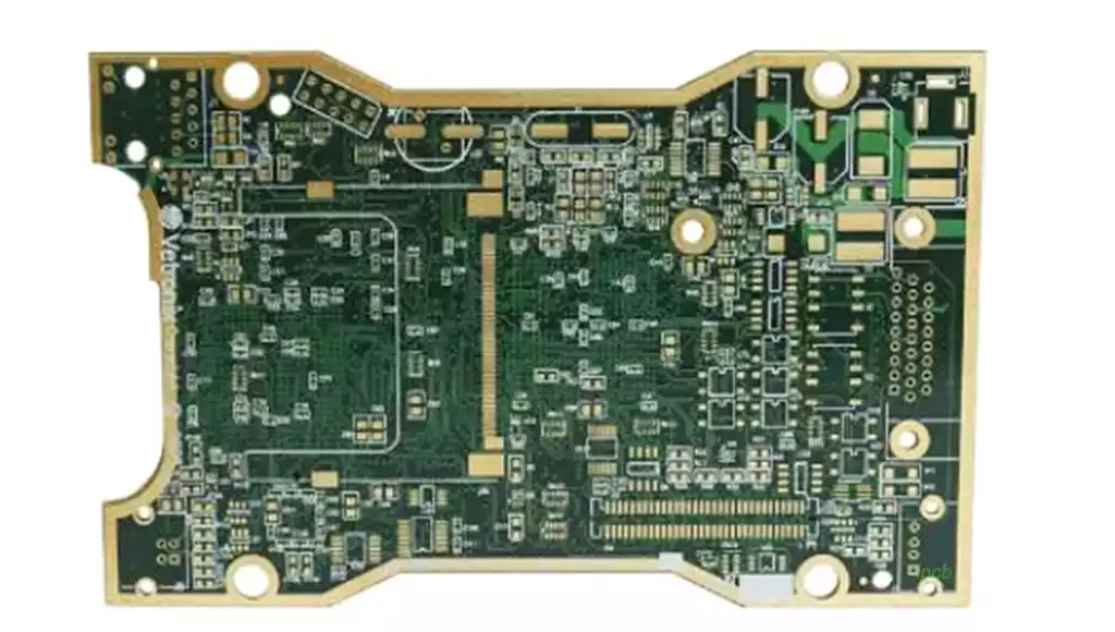
Soldermask is a layer of PCB oil that covers the copper wires and PCB material to insulate and protect the outside of the PCB from short circuits and the environment. But how to assemble own pcb solder mask?
How to assemble own pcb solder mask
Pre-cleaning: Before the soldermask process is implemented, the PCB surface must be thoroughly cleaned to remove oil, dust and other foreign matter to ensure that the soldermask can be firmly adhered to the PCB substrate.
Application of photopolymerized soldermask: Through screen printing or spraying technology, the photopolymerized soldermask is evenly covered on the PCB surface. This special liquid material hardens quickly under UV light.
UV irradiation molding: The coated PCB is fed into the exposure machine for UV irradiation. The exposure machine transfers the pattern to the PCB surface based on the soldermask pattern in the PCB design data, while the unirradiated soldermask remains in its original state.
Developing to remove uncured parts: After irradiation, the PCB needs to undergo a developing step to remove the soldermask that has not been hardened by the UV light. The developing solution is mostly alkaline, which effectively dissolves the uncured soldermask, leaving the cured pattern behind.
Enhanced Curing: After developing, the PCB undergoes a curing process to enhance the hardness and durability of the soldermask. This is usually done at elevated temperatures to induce cross-linking of the chemical components of the photopolymerized soldermask to form a solid polymer structure.
Quality Inspection and Correction: The cured PCB is subjected to a quality inspection to verify the integrity and accuracy of the soldermask. Any defects or errors found are repaired or reworked as necessary.
Subsequent processing: In some cases, the soldermask may require further processing, such as sanding, polishing, or applying protective coatings to improve its abrasion resistance and appearance.
Final Quality Verification: PCBs are subjected to rigorous inspection to ensure that the quality of the soldermask meets design specifications and industry standards.
Proper procedures and meticulous workmanship are crucial when assemble own PCB soldermask. Improper handling may result in poor board functionality and reduced reliability.
Common mistakes when assemble own pcb soldermask:
Uneven thickness of soldermask: Uneven thickness of soldermask will result in uneven flow of solder, which may trigger unstable solder joints or short circuit.
Soldermask peeling: In the PCB manufacturing process, if the adhesion between the soldermask and the copper substrate is not up to standard, it may cause the soldermask to fall off in subsequent processing or use.
Soldermask contamination: If the surface of the soldermask is covered with grease, dust and other contaminants, it will affect the soldering quality and may lead to soldering defects.
Soldermask cracking: The soldermask may crack under thermal or mechanical stress, affecting the overall reliability of the PCB.
Insufficient thickness of soldermask: Too thin a soldermask may not adequately protect the board, resulting in solder seeping into non-soldered areas.
Uneven color of the soldermask: Uneven color of the soldermask may be caused by uneven application of ink or uneven baking process, which may weaken its protective effectiveness.
Blurred edges of the soldermask: Poorly defined edges of the soldermask may result in solder spilling into non-soldered areas during soldering, triggering short circuits.
Bubbles in the soldermask: Bubbles may form in the soldermask during the curing phase, which will affect its surface flatness and protective properties.
Pinholes in the soldermask: Pinholes are tiny holes in the soldermask, which may become channels for moisture and pollutants to intrude, affecting the long-term stability of the PCB.
Soldermask and copper layer size mismatch: If the size of the soldermask and copper layer do not match, it may result in solder not being able to accurately fill the pad when soldering, thus affecting the overall quality of the soldering.

How to assemble own pcb solder mask need to consider the following aspects:
- Soldermask Material Selection: Soldermask is mainly made of a mixture of epoxy resin and pigment, and common colors include green, blue and red. When selecting, the material needs to be evaluated for heat resistance, chemical stability, abrasion resistance, and adhesion to the copper layer.
- Soldermask thickness setting: The standard thickness of soldermask is usually between 0.1 mm and 0.2 mm. If it is too thick, it may affect the heat distribution during soldering; if it is too thin, it may not provide sufficient protection.
- Layout design of openings: Openings are created in the soldermask for pads,test points,and other soldering areas.The size and shape of the openings should be designed according to the specific size and shape of the soldered components to ensure that the solder can flow smoothly into the pads during soldering.
- Soldermask extension processing: In order to avoid short circuits between the pad and the alignment,the soldermask layer will usually be around the pad to extend a certain distance, this distance is called “Soldermask Extension”.The specific size of the expansion should be based on the board’s layout density and component spacing to determine.
- Soldermask and alignment spacing: Soldermask and the alignment between the need to maintain appropriate spacing to prevent damage to the alignment of the soldermask in the production process. This spacing is usually controlled between 0.1 mm and 0.2 mm.
- Soldermask and component spacing: For mounting components, the spacing between the soldermask and the component also needs to be considered to ensure that the component will not collide or interfere with the soldermask during the mounting process.
- Soldermask graphic planning: the graphic design of the soldermask layer needs to match the layout and alignment of the circuit board to ensure that the overall aesthetics and functionality of the circuit board.
- Soldermask Production Control: During the production process, the soldermask coating process needs to be strictly monitored, including coating uniformity, thickness, and degree of curing to ensure the quality of the soldermask.
- Soldermask performance testing: After the completion of the circuit board production, the soldermask performance testing, including adhesion testing, wear resistance testing and thermal shock testing to ensure that the performance of the soldermask to meet the design requirements.
- Environmental protection material selection: With the enhancement of environmental protection awareness, the choice of soldermask materials also need to consider its environmental performance, to avoid the use of materials containing harmful substances.
In understanding how to assemble own pcb solder mask, we realize that every step of the process needs to be done carefully. From cleaning to curing to quality inspection, each step is essential. At the same time, we have learned to recognize and avoid common mistakes to ensure the quality and performance of the solder resist. Through continuous practice and learning, we are able to better master this skill and provide reliable guarantee for DIY electronic projects.


