In electronics manufacturing, PCB (Printed Circuit Board) paste reflow is a crucial process that determines the quality of the connection between the electronic components and the PCB board. Although specialised equipment is preferred in most cases, homemade PCB paste reflow is also a viable option for small batch production or experimental purposes. But how to assemble own pcb paste reflow.
How to assemble own pcb paste reflow
Choosing the right PCB:
The first consideration is to select a PCB that exactly matches the specifications of the product under test, including size, thickness, and material. If it is not possible to obtain an identical PCB, then an alternative board should be selected that is of comparable thickness and has the same dimensions of the key components under test.
Determine the layout of the temperature measurement points:
According to the distribution of components on the PCB board, size and the direction of entry into the reflow oven, to accurately set the location of the temperature measurement point. Generally, the highest and lowest temperature points on the board are selected as the key points for temperature measurement. For example, for a furnace that enters and exits from left to right, the highest temperature point may be located on an element in the upper right area, while the lowest temperature point may be located on an element in the lower left area.
Install temperature measuring wires:
Select a temperature measuring wire suitable for the reflow soldering operating environment,such as Type K Ni-Cr and Ni-Al alloy wire, which is typically 0.254 mm in diameter. Firmly fix the temperature measuring wire to the preset position on the PCB board,using auxiliary materials such as heat-conducting adhesive, red adhesive or high-temperature-resistant tin wire.
Create temperature measurement connection points:
Create connection points on the PCB board so that the temperature measuring wire and the oven temperature tester can be stably connected. Make sure that the connection points are strong enough not to fall off during reflow soldering.
Test and calibration:
Properly connect the completed temperature measurement board to the oven temperature tester. Test the board by placing it in the reflow oven, either on a bracket or directly on a conveyor belt. Collect oven temperature data and evaluate if the temperature profile meets the product design requirements.
Make adjustments and improvements:
If the test results do not meet standards, adjustments need to be made to the location of the temperature measurement points or connections. Repeat the test until accurate and reliable data is obtained.
Documentation and Confirmation:
Record the test procedure, results and all adjustments for future reference. Print and confirm the oven temperature profile sheet, sign it and keep it on file.
Reflow soldering operation process
Solder Paste Coating: Use coating equipment or solder paste printing equipment to evenly apply solder paste to the soldering area of the PCB.
Component placement: With the help of placement equipment, precisely place the electronic components on the PCB coated with solder paste.
Pre-heating process: The PCB is fed into the pre-heating area of the reflow soldering machine to evaporate the solvents in the solder paste and to gradually increase the temperature of the metal powder in the solder paste.
Main Heating Stage: The PCB is fed into the main heating zone of the reflow machine to rapidly melt the solder paste and fully fill the void between the pins and pads.
Cooling and curing: Remove the PCB from the reflow machine for natural cooling or assisted cooling with an air-cooling device to solidify the solder paste into a firm soldered joint.
Precautions and Tips
In the process of homemade reflow soldering, you should pay special attention to the following points:
Safety first: Ensure that the working environment is well ventilated to avoid inhaling fumes that evaporate during the soldering process, and be careful of hot surfaces to avoid burns.
Temperature control: Excessive temperatures can damage sensitive components, so be sure to make reasonable adjustments according to the nature of the solder paste and use a thermometer for accurate monitoring.
Appropriate wind speed: Excessive wind speed may result in an uneven flow of solder paste. Appropriate wind speed ensures even melting of the paste and avoids shifting of components due to high wind speed.
Multiple tests: Before formally using the equipment, it is recommended to carry out several test soldering to ensure the stability and reliability of the equipment.
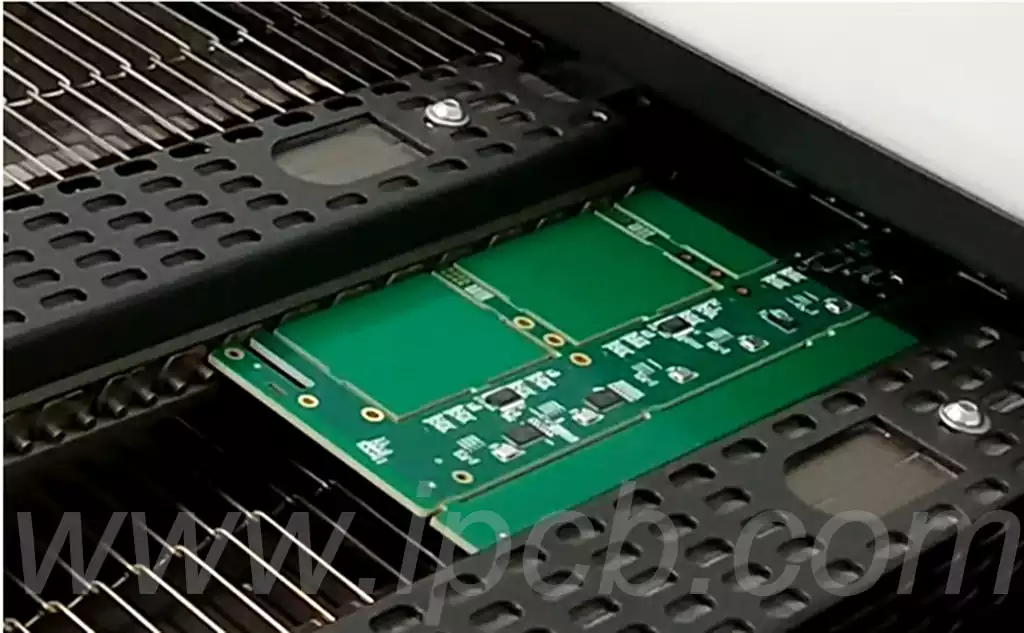
Common problems and solutions of how to assemble own pcb paste reflow
Bad soldering
In the reflow soldering process, poor soldering is one of the most common problems, which is manifested as false soldering or incomplete solder joints.
Solution:
Make sure to use high quality solder paste and apply it evenly to the pads.
Adjust the temperature setting of the heat gun or oven to ensure that the soldering temperature reaches the melting point of the solder paste, usually around 220°C.
Extend the heating time to ensure that the components and solder joints are sufficiently heated.
Short-circuiting of solder joints
A problem that usually occurs between neighbouring components, resulting in a broken or shorted circuit.
Solution:
Ensure that the right amount of solder paste is used to avoid excessive coverage of the pads.
Use nozzles of different diameters to control air velocity and reduce interference with solder joints.
Check the PCB design before soldering to ensure that the soldering position is well laid out to avoid excessive proximity between neighbouring solder joints.
Solder Balls or Bridges
Solder balls or bridges are small balls of solder that form during the reflow soldering process and usually cause short circuits as well.
Solution:
Ensure that the temperature control is precise and avoid excessive temperatures.
When using a hot air gun, maintain a reasonable heating distance (generally 5-10 cm) to reduce the impact of excessive heat flow.
Reasonable design for the soldering area to reduce the possibility of solder gathering.
Component Damage
High temperatures, excessive time or thermal stress may result in component damage during the soldering process.
Solution:
Ensure that the temperature profile meets the component’s specifications and avoid sudden temperature changes.
For sensitive components, know their temperature range in advance and adjust reflow settings accordingly.
If possible, use staged heating to slowly increase the overall PCB temperature to reduce thermal stress.
PCB Deformation or Warping
During the reflow soldering process, PCBs may be deformed or warped due to uneven heating or material quality issues.
Solution:
Select high quality PCB materials to reduce the risk of warping due to thermal stress.
Before heating, make sure that the hot air in the soldering area is evenly distributed, which can be achieved by reasonably arranging the position of the components and adding appropriate fixtures.
Strictly control the heating temperature and time to reduce the stress generated during heating.
By understanding how to assemble own pcb paste reflow,you can try to make homemade pcb solder paste reflow soldering and control the soldering process flexibly to improve the quality of soldering in small batch production or experimental projects.
