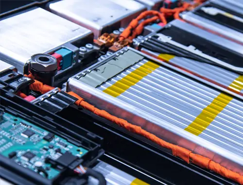
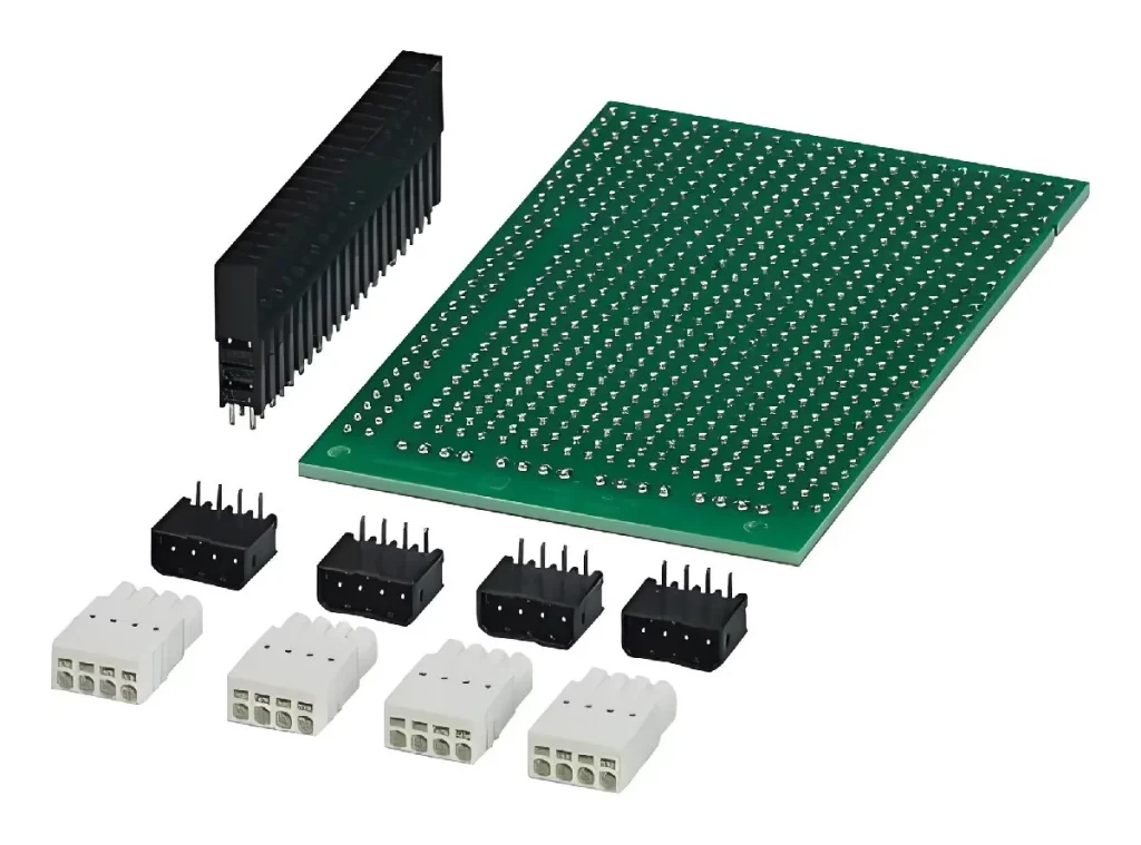
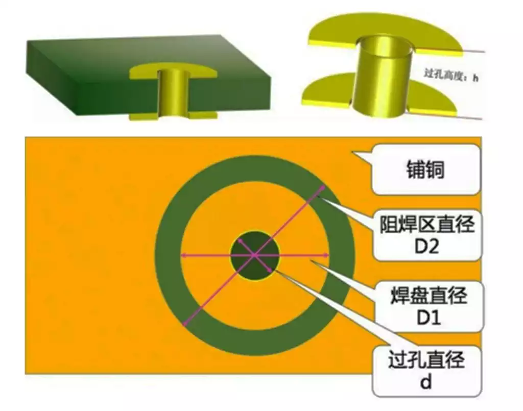
Cloning pcb board refers to the process of making circuit boards, assembling components and debugging circut boards on the basis of physical electronic products and their printed circuit boards through reverse engineering means of in-depth analysis of the circuit boards to accurately recover the original product documents, bill of materials, circuit schematics and other key technical documents, and then based on these technical documents and production information, to make circuit boards, component assembly and pcb board debugging to reproduce the original printed circuit boards in their entirety.
1.Get a PCB board, the first task is to exhaustively record on paper all the components of the model, specifications and their specific location, pay particular attention to the diodes, transistors, and the direction of the integrated circuit chip chip notch direction. At the same time, use a digital camera to take two photos of the component layout for reference.
2.Remove all components and remove tin from the pad holes. Next, clean the board thoroughly with alcohol and place it in the scanner, increasing the scanning resolution appropriately when scanning to obtain a clear image of the pcb board. Afterwards, use water sandpaper to gently polish the top and bottom layers of the circuit board, until the copper film surface is bright, and then put it into the scanner again, using PHOTOSHOP software to scan the two layers in colour mode. During this process, be sure to ensure that the PCB in the scanner placed correctly, otherwise the scanned image will not work properly.
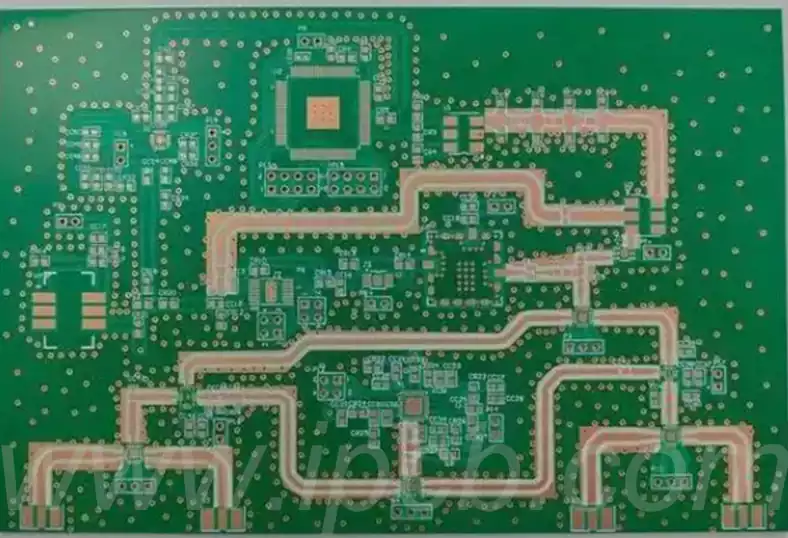
3.In PHOTOSHOP to adjust the contrast and brightness of the image, so that the copper part of the film and non-copper part of the formation of a sharp contrast, and then convert the image to black-and-white mode, and double-check the clarity of the lines. If it is not clear, it is necessary to continue to adjust; if it is clear, the image will be saved as two files in black and white BMP format. If you find that there are problems with the image, you also need to use PHOTOSHOP to make the necessary corrections.
4.The two BMP format files were converted to AD (such as Altium Designer and other electronic design automation software) can be recognised format. Import the two layers in AD, if the two layers of pads (PAD) and over-hole (VIA) position of the basic coincidence, it shows that the previous steps are completed well; if there is a deviation, it is necessary to repeat the third step until the complete match. Next, the top BMP file into a TOP.PCB file, pay attention to the conversion to the silk screen layer (SILK layer, usually yellow), and then tracing the line on the layer, and according to the second step of the drawing placed components. After completing the tracing, delete the SILK layer, repeat the process until all layers are drawn.
5.Merge the TOP.PCB and BOT.PCB files in AD to form a complete circuit board diagram. Next, use a laser printer to print the top layer (TOP LAYER) and bottom layer (BOTTOM LAYER) onto a transparency film at a 1:1 ratio. The film will be covered in the original PCB board for comparison, if there is no error, it indicates that the reproduction is successful.
In view of the electronic products mainly through various types of circuit boards to achieve control functions, therefore, through the clone pcb board this process, you can extract a full set of technical information of any electronic product, and to achieve product imitation and cloning.
