Static electricity arises from the separation of charges that occurs when two different materials come into contact with each other or are rubbed together, causing an object to become electrically charged as a whole. For example, the constant friction of people wearing clothes, or even the simple act of tearing paper, can trigger the generation of static electricity. In the manufacturing process of electronic products, the choice of materials, environmental conditions and personnel operating behaviour and other factors, can become the source of static electricity, and thus the stability of electronic products constitute a potential risk.
The impact of static electricity on the PCB board should not be ignored, it may interfere with the stable operation of electronic products, affecting its thermal efficiency and shorten the service life. Specifically, the components on the PCB board may be damaged due to electrostatic action, the insulating layer is broken and the phenomenon of instantaneous release of large amounts of energy, accompanied by the generation of radiated noise, these are static electricity on the PCB board poses a threat to the direct performance.
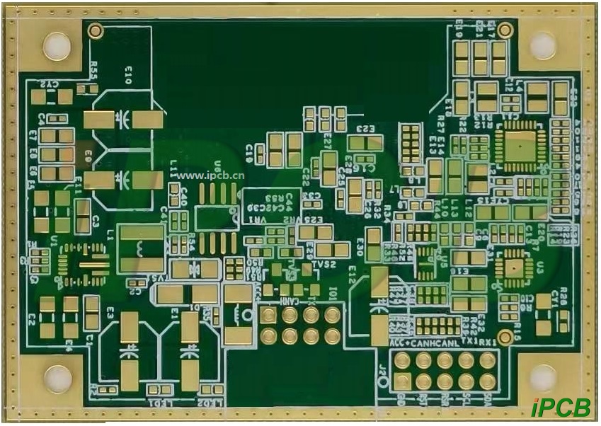
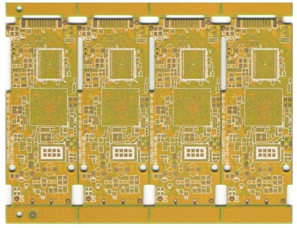
PCB anti-static measures:
- Grounding design
Grounding design: PCB anti-static strategy is the most important, proper grounding design can ensure that the static electricity effectively into the ground, for the circuit board to provide protection for electronic components.
Multi-point grounding: By setting up multiple grounding connections on the PCB to accelerate the process of static dissipation, especially in multi-layer board design, can effectively reduce the resistance and inductance effects.
Expanded grounding layer: increase the area of the grounding layer, commonly used in multilayer PCB design, the use of copper foil laying to enhance the grounding effect, further weakening the electrostatic interference.
Dedicated protective grounding: Configure an independent grounding path for static-sensitive components to avoid interference from other circuits. - Electrostatic suppression components
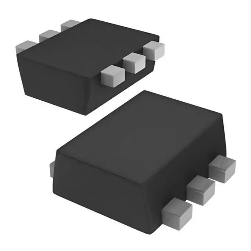
Integrated static protection components: PCB design into a specific component to resist electrostatic damage to the circuit and components.
ESD Diodes: Installed near sensitive components to effectively consume and disperse electrostatic charges and protect components from damage.
Discharge Capacitors: Added to input/output ports to provide a rapid release path for static electricity.
Current limiting resistor: added in the signal path to limit the current strength during electrostatic discharge and protect circuit components. - Optimise device layout to reduce the impact of static electricity
Layout strategy: through careful layout, reduce the potential threat of static electricity on sensitive components, reduce the overall circuit board electrostatic interference.
Internal placement of sensitive components: Avoid placing electrostatic sensitive components on the edge of the PCB, because it is easy to gather static electricity area, the inner layout is safer.
Input and output isolation: Set up isolation zones between input and output ports and sensitive components to block the spread of electrostatic interference.
Partition layout: analogue, digital and power supply circuits are partitioned to reduce the signal interference caused by static electricity. - Avoid sharp corner conductor design to mitigate electrostatic problems
Smooth wiring: Use curved wiring instead of right-angle turns to reduce the possibility of electrostatic build-up.
Uniform wiring principle: Maintain the consistency of line width and spacing in the dense wiring area to avoid static accumulation caused by uneven electric field. - Increase the isolation protection area to isolate the static sensitive components
Establishment of protective areas: set up protective barriers around the critical areas or interfaces of the PCB to prevent direct intrusion of electrostatic charges into sensitive circuits.
Protective ring design: around the critical areas or interfaces arranged around the protective ring, effective isolation of static electricity.
Shielding layer application: additional shielding layer or shielding cover in sensitive areas to weaken the impact of static electricity on the circuit. - Verification tests of electrostatic protection design
Comprehensive testing: comprehensive assessment of the anti-static design of the PCB to ensure that it meets the established anti-static requirements.
Static electricity test: through the simulation of different strengths of static electricity, check the response of the PCB board, and accordingly adjust the optimisation of circuit design.
Contact and air discharge test: simulate human operation, interface plugging and air electrostatic discharge, respectively, to verify the design of the electrostatic protection effect, to ensure the high reliability of the design.
The anti-static design of the PCB has a significant effect on mitigating static damage, enhancing the overall stability of the board and extending its service life. With proper grounding layout, integrated electrostatic protection components, and optimised device arrangement and other means, PCB can significantly improve its electrostatic protection performance, widely used in those sensitive to static electricity and require high precision electronic equipment.