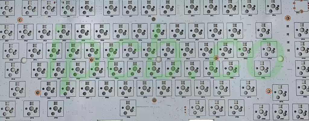
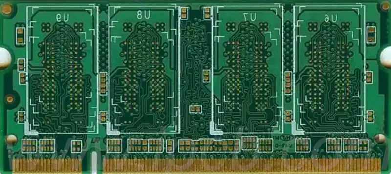
PCB circuit board infrastructure is equivalent to a building’s foundation and framework, which consists of four main layers: top layer (Top Layer), bottom layer (Bottom Layer), inner layer (Inner Layer) and pad layer (Solder Mask Layer).
Top signal layer (Top Layer)
This layer as the PCB circuit board ‘front’, mainly for the layout of electronic components. In double-layer and multilayer board design, the top signal layer is also responsible for wiring to ensure that the circuit is unobstructed.
Mid Layer
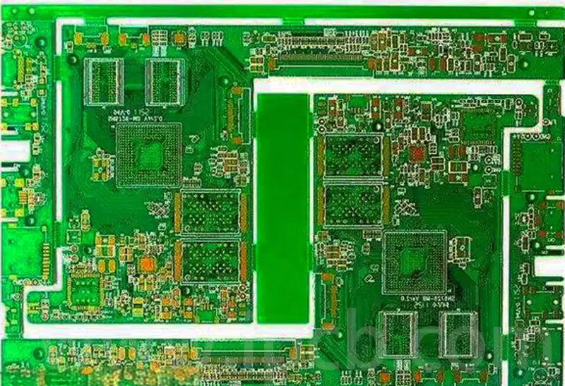
As the ‘heart’ of a multilayer board, the mid signal layer, which can number up to 30 layers, is the main area for wiring. These layers are intricately interwoven within the board, providing ample space for complex circuit designs.
Bottom Signal Layer (Bottom Layer)
As the ‘cornerstone’ of the PCB circuit board, the Bottom Signal Layer is not only used for wiring, but is also often used as a substrate for soldering components. Its design has a significant impact on the board’s robustness and durability.
Top Screen Printing Layer (Top Overlayer)
This layer can be regarded as the PCB’s ‘identity mark’, which is labelled with key information such as the outline, number and parameters of the components. These markings for the assembly and maintenance of the circuit board is essential.
Bottom Overlayer
Similar to the Top Overlayer, the Bottom Overlayer is used for labelling component information. The Bottom Overlayer can be omitted if the Top Overlayer contains all the necessary information.
Internal Plane
The internal power layers act as the ‘power core’ of the PCB circuit board, covering the power supply, reference power and ground planes. They provide a stable power supply and signal reference for the circuit, which is a key factor to ensure the stable operation of the circuit.
Mechanical Layer
This layer defines the physical characteristics of the PCB circuit board, such as board shape, size and other parameters. It is an integral part of the circuit board manufacturing process.
Solder Resist Layer (Solder Mask)
Solder Mask acts as a ‘protective barrier’ for the PCB circuit board, covering the pads and vias to prevent short circuits and contamination during the soldering process. The top and bottom solder masks together form the soldering surface of the board.
Paste Mask
The Paste Mask is critical to the soldering of SMD components and determines where the solder paste is printed. The design of this layer is directly related to the quality and reliability of soldering.
No wiring layer (Keep Out Layer)
This layer as a PCB design ‘no-fly zone’, a clear boundary of the wiring. In the prohibited wiring layer, any line with electrical characteristics are not allowed to cross to ensure the safety of the circuit.
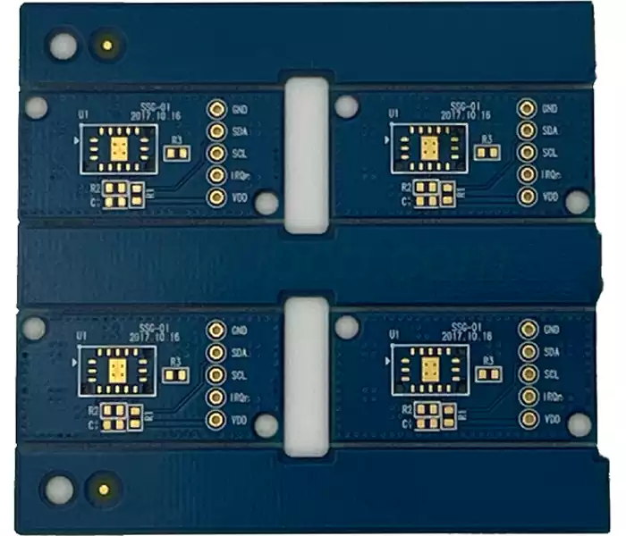
Multi Layer
As a ‘link’ in PCB design, Multi Layer connects different layers of the board through via holes or through-hole pads to achieve a three-dimensional design of the circuit.
Drill Layer
The Drill Data Layer serves as a ‘construction drawing’ for PCB manufacturing, providing information on the precise location and size of drilled holes. This layer plays a vital role in the assembly and functional realisation of the circuit board.
Classification and Application of PCB circuit boards
According to the number of layers, PCB circuit boards can be divided into single-layer boards, double-layer boards and multilayer boards:
Single-layer board: only one layer of conductive copper foil, simple structure, suitable for some low-cost electronic products.
Double-layer boards: there are two layers of conductive copper foil, connected by through-holes, suitable for slightly more complex circuits.
Multi-layer boards: usually have more than four layers of conductive copper foil, the number of layers can be dozens of layers.
Selecting the right semiconductor board is a complex and significant decision-making process that involves weighing a number of factors.
First and foremost, the board’s application environment must be clearly defined. If it is used in high-performance computing scenarios, it is necessary to select semiconductor boards with high-speed data transmission and low-latency characteristics to ensure that data can be processed quickly and efficiently transmitted. In the field of artificial intelligence, for example, in view of its stringent requirements for computing speed and accuracy, should be selected to integrate cutting-edge processors and high-speed interface board.
Secondly, power consumption considerations should not be ignored. For portable devices or applications with strict limits on power consumption, such as IoT devices, low-power semiconductor circuit boards become a must. This extends the battery life of the device and improves the user experience. In this process, it is necessary to pay close attention to the power consumption of the chips on the board and the performance characteristics of the power management system.
In addition, compatibility should not be underestimated. Ensure that the selected semiconductor board is seamlessly compatible with other hardware components (e.g., processor, memory, etc.) to prevent mismatches that could lead to system failures or performance degradation. At the same time, the board’s scalability needs to be considered, so that it can be easily expanded in the event of future upgrades or new functionality.
Finally, the cost factor also needs to be taken into account. According to the project budget and the actual needs of the project to find the best balance between performance and cost. Do not ignore the quality and performance of the board just because of the pursuit of low prices, and should not be over-invested funds, resulting in unnecessary cost waste.
Each layer of the PCB circuit board infrastructure has its own role to play, to build a solid foundation for the stable operation of the circuit. Selection of semiconductor circuit boards when the comprehensive consideration of many factors, in order to select the appropriate choice. In the future, PCB technology is expected to continue to innovate, for the development of the electronics field to bring more surprises.