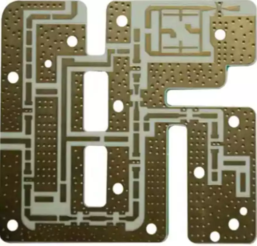
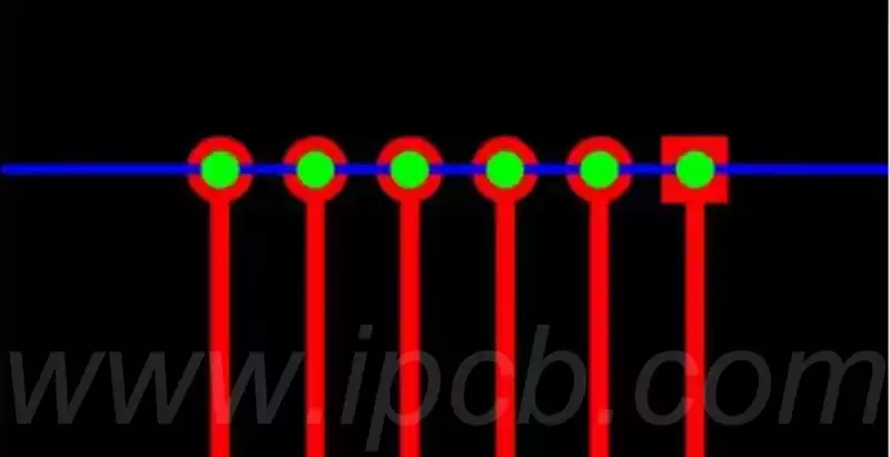
Plated half holes are similar to plated through-holes, but occupy only half of the vertical space. This design makes them structurally more compact while maintaining good electrical and mechanical connectivity. Through soldering, these half-holes can connect individual PCB modules to the motherboard, providing superior joint access and coaxial alignment over conventional pads.
Plated half hole process seems to have completed the metallisation of the holes in the implementation of half-cutting operations, only in the conventional PCB processing process can be added at the end of the milling profile process, but in fact there are many technical points and process control requirements are extremely high. Process Flow.
Precision tool path planning
The plated half hole cutting adopts a double V-track tool path, through the optimisation of the tool path to ensure that the force on both sides of the hole wall is uniform, to avoid the deformation or burr caused by unilateral cutting.
Optimisation of second drill pre-processing
Additional guide holes are installed at the edge of the broken holes, the copper skin is stripped in advance to reduce the cutting resistance, a slotting knife is used instead of the traditional drill, and the spindle speed and feed speed parameters are adjusted to achieve clean cutting without burrs.
Enhancement of copper plating process
The whole plate plating is implemented on the substrate to form a conductive copper layer of uniform thickness on the hole wall, which provides a reliable conductive foundation for subsequent line production.
Outer line composite plating
After pressing film, exposure, development, the second copper plating on the substrate to thicken the copper layer, and synchronous tin plating to form a corrosion protection layer, to ensure that the hole wall copper layer and the outer copper layer to form a complete electrical connection.
Plated half hole moulding control
High-precision cutting equipment is used to accurately divide round holes into half-hole structures, and the cutting process requires strict monitoring of tool wear and cooling parameters to avoid copper layer stripping.
Anti-Plating Removal
Chemical de-filming process is used to remove the residual anti-plating layer during the pressing process and restore the activity of the copper surface.
Etching precision control
Selective etching is carried out to remove the exposed copper surface after film removal, etching solution concentration, temperature and etching time need to be precisely controlled to prevent over-etching or under-etching.
Tin layer stripping
Adopt environmentally friendly tin stripping process to remove the tin layer on the hole wall to ensure that the copper surface finish meets the subsequent process requirements.
Post-processing enhancement
Red tape is used to fix the unit board after forming, and the second deburring is carried out through alkaline etching line to improve the quality of the edge of the aperture.
Copper-tin composite protection mechanism
Half-hole cutting is carried out after secondary copper and tin plating to protect the structural integrity of the copper layer by using the tin layer, and the copper layer forms a strong bond with the copper surface of the substrate during the cutting process, effectively preventing the copper layer from peeling off or warping.
Closed Loop Yield Improvement
Half-hole forming after the implementation of the sequential removal of film, etching process, through the process sequence optimisation to avoid copper surface oxidation, to eliminate residual copper and short-circuit defects, and ultimately achieve a significant increase in the yield of the metallization of half-hole PCB.
PCB plated half hole process difficulties:
Accuracy of design documents
In PCB plated half hole processing, the accuracy of the design document plays a decisive role. If there are defects in the design file or deviation from the actual production standard, it will directly cause the quality of half-hole processing. For example, in the graphics rendering, plate processing, plating process and other aspects of the error, it is very easy to cause half-hole aperture overshoot or deformation and other problems. Therefore, it is necessary to ensure that the design documents are accurate and in full compliance with the actual production specifications.
Precise control of the process
PCB plated half hole processing process has a high degree of complexity, need to invest a lot of time and energy to carry out refined operation, and maintain high processing accuracy. Any operation negligence may lead to aperture size deviation, uneven quality of the aperture wall, circuit path damage, repeated openings and other quality problems, which in turn affects the quality of the finished product of half-hole processing.
Strict control of material quality
Material quality has a critical impact on the PCB plated half hole processing effect. In the material selection and application stage, we must fully consider its chemical properties matching, process compatibility and scope of application and other core elements. If the purity of the material is not enough or the composition ratio is unbalanced, it is very easy to lead to half-hole processing effect is not up to expectations, and even irreversible quality defects.
Standard guarantee of equipment and technology
In order to ensure that the quality of PCB plated half hole processing standards, we must ensure that the technical parameters of the production equipment in line with the process standards, and the establishment of regular testing of the state of the equipment and maintenance of wearing parts mechanism. When the technical parameters of the equipment deviates from the standard or faulty operation, will significantly reduce the processing efficiency, hindering the normal advancement of the overall production process.
In the process of PCB plated half hole processing, it is necessary to systematically guarantee the accuracy of the design documents, the precision of the process, the reliability of the material quality and the stability of the equipment technology. Only through a full range of pre-control measures and standardised management, in order to effectively avoid all kinds of risks in the processing. At the same time, the establishment of a standardised production management system is equally important to protect the processing quality and improve production efficiency.
PCB plated half hole process as a key technology in the field of modern electronics manufacturing, not only carries the realization of high-density, miniaturised circuit design mission, but also on the processing accuracy, material quality and equipment technology puts forward stringent requirements. Looking to the future, with the continuous innovation of electronic technology and the continuous upgrading of market demand, PCB half-hole process will face more challenges and opportunities.