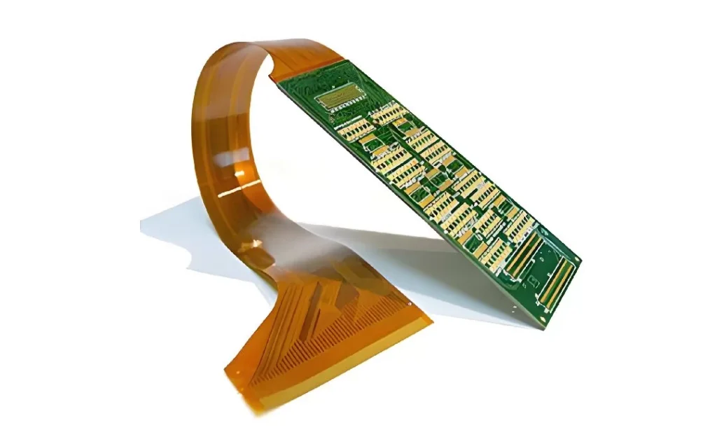
In the rapid development of electronic technology, power supply pcb as one of the core components of electronic equipment, its design quality is directly related to the stability and safety of the entire system. In the design process of power supply PCB, slot hole design as a key technology, not only affects the electrical performance of the circuit board, but also related to the product’s heat dissipation effect, mechanical strength and the ability to comply with international safety standards.
Why are there slotted holes on power supply pcb?
- Regulatory requirements on creepage distance
Creepage distance refers to the shortest path distance between two conductive parts measured along an insulating surface, or between a conductive part and the protective interface of a device. In the power supply printed circuit board (PCB) design, in view of the co-existence of high-voltage devices and low-voltage devices, in order to ensure electrical safety, the two types of devices need to be isolated. When conventional design is difficult to meet the minimum creepage distance standard, cut slot operation becomes a common solution strategy. By cutting grooves, high-voltage areas and low-voltage areas can be efficiently isolated to ensure electrical safety. - Isolation measures for high-voltage areas
In the layout of power supply pcb, high-voltage areas are usually prohibited in all layers of copper laying operations to ensure safety. As an effective means of isolation, cutting grooves can draw clear boundaries between the high-voltage area and the low-voltage area, thus reducing the electrical risk and improving the overall safety. - Optimisation strategy of electrical gap
Electrical clearance refers to the shortest spatial distance between two conductive components, or a conductive component and equipment and its easy-to-contact surface. In some specific cases, due to PCB layout limitations, the electrical gap may not meet the established requirements. In this case, through the opening of slots in the appropriate location, you can adjust and optimise the electrical gap, thereby improving electrical performance and ensuring the stable operation of the circuit. - Risk Reduction and Reliability Improvement
Optimizing creepage distance by slotting design can not only significantly reduce the electrical risk, but also effectively improve the reliability of the power supply PCB. In the case of space conditions allow, the appropriate increase in creepage distance helps to further reduce the risk, improve the safety performance of the equipment, and provide a strong guarantee for the long-term stable operation of the circuit. - Key points of slotting design
In the grooving design, special attention should be paid to the width of the groove. Generally speaking, the width of the slot should be greater than 1mm to ensure the effectiveness of its isolation effect. In addition, the location and number of slots also need to be carefully designed according to the specific PCB layout and electrical requirements, to avoid adverse effects on the overall structure and performance of the PCB, to ensure the rationality and stability of circuit design.
Power supply pcb above the role of the slot hole
Power supply pcb above the slot hole is mainly used for electrical isolation, fixed components, ventilation and heat dissipation and improve circuit stability.
Electrical isolation: Slot holes on the PCB board to create physical isolation, to avoid electrical signals interfere with each other, to ensure the safe operation of the circuit.
Fixed components: Through the installation of screws or nuts through the slot holes, electronic components or mechanical parts are firmly fixed on the PCB board to enhance the stability of the structure.
Ventilation and heat dissipation: Slot holes help to dissipate heat, preventing electronic components on high-power circuits from being damaged due to overheating and improving the reliability of the circuits.
Improve circuit stability: Slot holes can be used for grounding, eliminating noise in electrical signals and reducing the effects of electromagnetic interference, thus enhancing circuit stability and reliability.
Meets safety regulations: In the power AC input and AC and control level sections, the slotted holes ensure sufficient safety spacing to prevent creepage and meet safety regulations.
Design Flexibility: The design of the slotted holes allows greater flexibility in the layout and wiring of the PCB board, which can be adapted to different circuit requirements and component arrangements.
Structural Requirements: In the production of PCBs, it is sometimes necessary to cut slots in the corresponding positions to match the mould to meet specific structural requirements.
Adjustment of Creepage Distance: Slot holes are used to adjust the creepage distance between high voltage and low voltage parts to ensure the safe operation of circuits, especially when the voltage is high or the pollution level is high.
How to design power supply pcb slot holes?In PCB design, ensure the following points:
- Copper is prohibited on all layers in the high voltage area: avoid copper foil in the high voltage area to minimise the risk of conductivity.
- High-voltage and low-voltage sections need to be clearly demarcated: Define the boundary between high-voltage and low-voltage areas.
- Maintain minimum creepage distances: Calculate and maintain adequate creepage distances based on operating voltage and other parameters.
- Slot hole width generally need to be greater than 1mm: to ensure that the width of the slot hole is sufficient to provide effective isolation.
Slotting during the PCB design process requires the following considerations
By placing the drilled holes
It is standard practice to place drill holes in the drill layer and load the processing information directly into the board file. This method is generally applicable to rectangular, square, round and other relatively regular slotting.
(1) Execute the menu command ‘Place – Pad’ to activate the command of placing pads, press the ‘Tab’ key in the state of placing, set the properties of the drill holes as shown in the figure, and place a slot with a width of 2mm and a length of 10mm.
Slot-Hole Size: the size of the hole, set it to ‘2mm’.
Slot-Length: the length of the slot, set to ‘10mm’.
③ Slot-Rotation: the angle adjustment of the slot, fill in according to the actual situation.
④ Slot-Plated: check the box when it is metallised and remove the check box when it is not metallised.
⑤ Simple- (X/Y): the size of the pad.
(2) Place a 5mm×5mm circular gouge and fill in the data information as shown in the figure.
So, the regular dugout slot such as rectangle, square, circle, etc. can be done by placing a drilled hole.
Through the board frame layer and board cut slot
Because pads cannot be set with shaped slot holes, shaped gouges cannot be processed by the above method. For shaped grooves, you can place the groove information to the board frame layer, note that it must be the selected board frame layer, and indicate it clearly to the board manufacturer, execute the menu command ‘Placement – Line’, and draw a desired shape of the closed groove in the board frame layer: Select the closed groove, and execute the menu command ‘Tools – Convert – Create from Selected Elements’. Transform – Create Board Cutout from Selected Elements’, create a cutout and switch to 3D to see the result.
Power supply PCB slot design, as an important part of the circuit board design, not only about electrical safety and performance stability, but also to ensure that the product meets international safety standards, to enhance market competitiveness of the key. With the continuous development of electronic technology, power supply PCB design will face more challenges and opportunities. As circuit board designers, we should continue to explore new technologies, new methods, innovative design concepts to lead the industry’s development trend, for the safe, stable and efficient operation of electronic products to contribute their own strength.