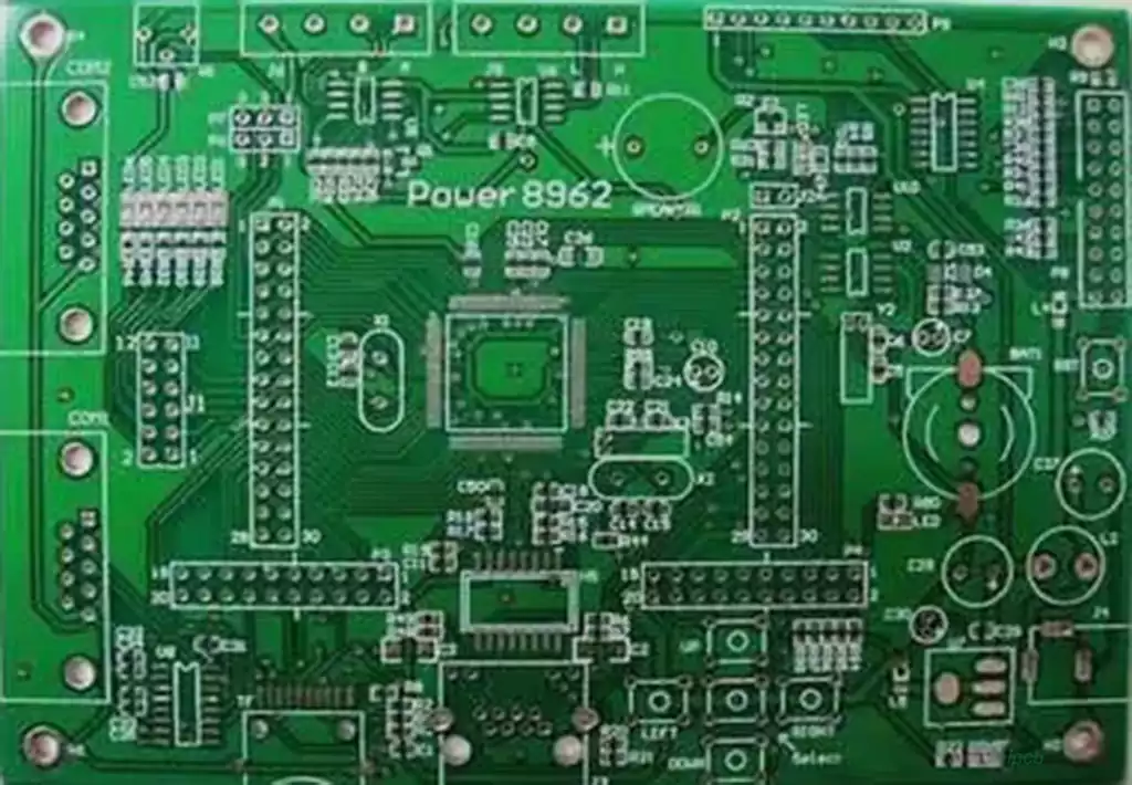
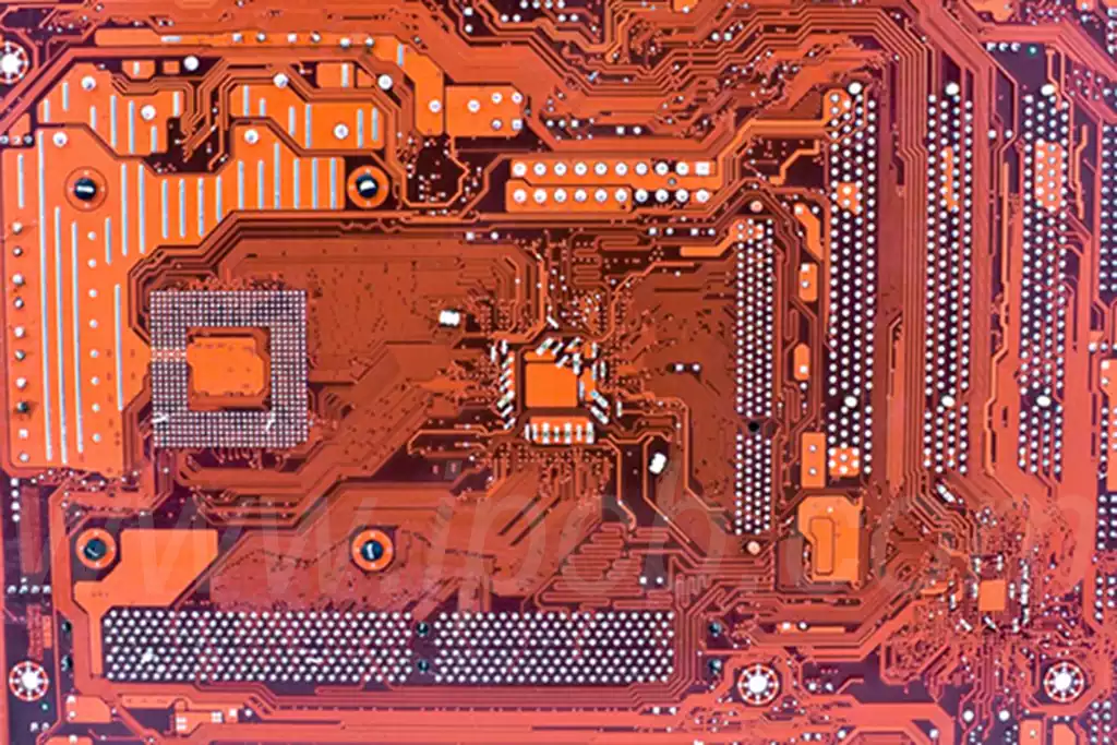
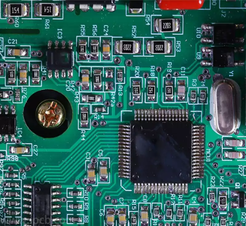
PCB Inspection is a comprehensive inspection of a printed circuit board that includes cosmetic, dimensional, solder joint, component mounting, electrical and functional testing. These steps ensure that the PCB is undamaged, meets design specifications, is well soldered, components are properly installed, circuits are properly connected, and overall functionality is proper. This helps to improve the quality and reliability of the PCB, ensuring its stability and performance in the final product.
PCB Inspection Items:
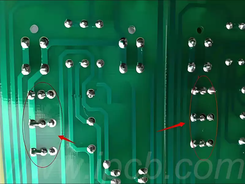
Press-Fit: The quality of the lamination is critical to the life of the PCB, and laminate peeling can lead to direct board functionality problems. Typically, laminate testing is used to examine the ability of a laminate to resist peeling under stress or heat.
Hole Wall Quality: Hole walls are typically analyzed in cyclic and rapid temperature change environments to understand their response to thermal effects and to ensure that the PCB is put into service without cracking or delamination of the hole walls.
Copper Plating: Copper foils on printed circuit boards are used to provide electrical conductivity and are tested for their quality, analyzed in detail for tensile strength and elongation. Cleanliness: Cleanliness relates to the board’s ability to withstand environmental factors such as weathering, corrosion and humidity.
Solderability: Materials are tested for solderability to ensure that components can be securely attached to the board and to prevent solder defects in the final product.
Electrical Testing: Conductivity is critical for PCBs, as is the ability to measure the PCB’s minimum leakage current.
Environmental testing: The main test of PCB performance and quality changes when operating in a humid environment, usually before and after the PCB is placed in a humid environment for weight comparisons, if the weight change is too large, it will be judged as scrap.
Purpose of PCB Inspection:
Ensuring quality, saving labor and clarifying defect criteria
The core objective of PCB inspection is to guarantee the quality of the products manufactured and to ensure that they are free of defects in their appearance. With automated inspection technology, labor savings can be achieved. Although the proportion of inspectors in factories is still high, the defects detected are mostly limited to functional defects. However, non-functional defects such as deformation, discoloration, or damage are also necessary. Therefore, it is important to set reasonable defect inspection standards in order to achieve the efficient use of the inspection system, to ensure product quality and reduce production costs of the three organic unity.
Strengthen the rigor of PCB inspection
PCB inspection needs to achieve a certain degree of rigor. To end-consumer products, for example, because of the cost of extremely stringent requirements, this time the inspection focuses mainly on the product’s minimum functionality to ensure. For the application of railroads, financial systems and aviation equipment and other areas of the product, because of its adverse consequences may have a significant impact on society, so it must be rigorous inspection. These products are relatively costly, and in order to ensure high reliability, it is necessary to detect potential defects that could lead to product failure. For this reason, inspections are conducted not only under regular use environments, but also under conditions that increase the use voltage, and resistors are examined with precision. In addition, rigorous inspection of the appearance of intermediate products is an effective way to eliminate potential defects.
Enhancing Product Conformity and Strengthening Engineering Control
Inspection is not only a key part of ensuring the final quality of the product, but also an important step in improving the product qualification rate. If an inspection system is introduced in the middle of the manufacturing process, it can effectively prevent defective products from flowing into subsequent processes. If defective products are found at the final stage of manufacturing, they can only be scrapped, after all, these products are manufactured through a number of processes.
In addition, based on the results of the intermediate stage of the inspection of the manufacturing process status analysis, can assess the strengths and weaknesses of the manufacturing process. If the poor performance of the process to take appropriate measures, you can make the process to maintain the best state.
Types of PCB inspection tools
- Magnifying glass: used to observe the circuit board on the small components and lines, to help inspectors find defects and problems. 2.
- Multimeter: Used to measure the circuit board voltage, current and resistance and other parameters, to determine the working status of the circuit board.
- X-ray detector: utilizing the principle of X-ray perspective, to detect whether there are breaks, missing and other problems inside the circuit board.
- Soldering iron soldering test: by soldering and disassembling certain components, detecting the connectivity and pass-through of the circuit board.
- Automatic tester: using sensors and computer technology to automate the testing of circuit boards with high efficiency and precision.
The function and use of various testing tools
- magnifying glass: simple to use, observation needs to maintain the distance between the eyes and the observation surface, adjust the angle of the lens, in order to see the circuit board more clearly.
- multimeter: a variety of functions, can be used to measure voltage, current and resistance and other parameters. The use of circuit boards need to be based on the actual situation to choose the appropriate range.
- X-ray detector: the use of X-ray perspective circuit boards, can detect whether there are internal fractures, missing and other issues. When using the need to pay attention to radiation radiation, comply with relevant regulations and requirements.
- Soldering iron test: by soldering and disassembling certain components, to detect the circuit board connectivity and on-off situation. Certain operating skills and experience are required to ensure the accuracy and reliability of the test results.
- Automatic Tester: Uses sensors and computer technology to perform automated testing of circuit boards. According to the set procedures and standards, the circuit board is comprehensively tested and analyzed.
In the wave of rapid development of the electronics industry, PCB inspection is an indispensable and solid line of defense to protect product quality. With comprehensive testing and advanced tools, we accurately control quality and enhance product competitiveness. In the future, with the technological innovation, PCB inspection will continue to upgrade, for the electronics industry’s steady march forward.