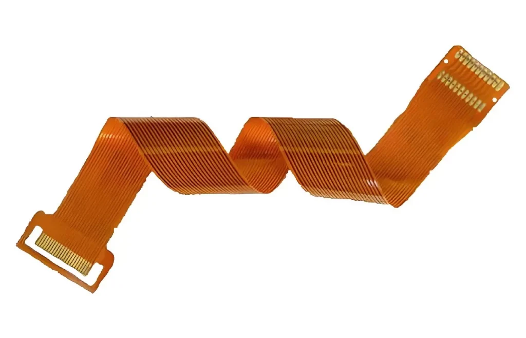
Flexible Printed Circuits (FPC) as electronic equipment thin and highly integrated core carrier, its welding technology directly affects product performance and reliability.
Common soldering methods for flexible circuit boards:
Thermocompression Soldering
Thermocompression Soldering as a FPC (Flexible Printed Circuits) flexible boards, a mainstream connection process, the core mechanism is the use of heat and mechanical pressure synergistic effect, prompting the conductive adhesive material to undergo the process of melting – curing, so as to achieve a reliable electrical connection between the metal conductor and the substrate. This technology is particularly suitable for the mass assembly of large-size flexible circuits due to its three main advantages – high soldering rate, high strength mechanical bonding, and large contact surface conductivity.
The process consists of three stages of precise control: firstly, the FPC and PCB (printed circuit board) are stacked on a pre-heated platform, so that the adhesive layer reaches the softening threshold through heat conduction; then set pressure is applied to ensure that the conductor and the pads form a microscopic level of adhesion; and ultimately, molecular-level curing is completed at a controlled cooling rate. The whole process requires strict control of the temperature profile (usually 180-220°C) and pressure parameters (0.2-0.8MPa), any parameter deviation may lead to defects such as false soldering, adhesive layer bubbles or substrate deformation.
Hot Air Soldering
Hot air soldering, as a key process in the field of precision electronics manufacturing, has a core mechanism of non-contact heat transfer through directional hot air flow, prompting the conductive colloid to complete the melting-curing process in a controlled temperature field, and then establishing a stable electrical connection between the metal conductor and the substrate. The technology is particularly suitable for precision assembly of large-size flexible circuit boards (FPCs) due to its three significant advantages – high-efficiency thermal response rate, wide-range uniform heating capability, and precise temperature gradient control.
The process includes three stages of precision control: firstly, the FPC and PCB with pre-set conductive adhesive are accurately aligned, and the soldering area is locally heated through a directional hot air system (adjustable temperature range of 150-250°C), so that the adhesive reaches the state of active softening; followed by the application of dynamic pressure (0.1-0.5MPa) to ensure that the conductor and the pads form a molecular-level bonding interface; and ultimately, in the programmed cooling Finally, the curing is completed under the programmed cooling curve (cooling rate ≤5℃/s). The whole process requires strict control of the hot air temperature field distribution (temperature uniformity ± 5 ℃) and pressure dynamic balance, any parameter deviation may lead to the adhesive layer porosity abnormality, insufficient interfacial bonding strength or thermal damage to the substrate and other defects.
Ultrasonic welding
Ultrasonic welding as an important branch of the field of advanced micro-connectivity technology, the core mechanism lies in the high-frequency mechanical vibration energy (frequency range of 15-70kHz adjustable) to achieve non-thermal material modification, prompting the conductive colloid in the ultrasonic cavitation effect of the completion of the melting – curing process, and then build the nanoscale bonding interface between the metal conductor and the substrate. This technology is particularly suitable for the high-precision assembly of miniature flexible circuit boards (FPCs) due to its three significant advantages – ultra-high-speed response (single-point soldering cycle time <0.5s), micron-level positioning accuracy, and zero-heat-affected-area characteristics.
The process includes three stages of precision control: firstly, the pre-coated conductive adhesive FPC and PCB are accurately positioned in the ultrasonic welding tooling, and then high-frequency vibration is applied to the welding area through the ultrasonic transducer (with an adjustable amplitude range of 10-50 μm) to make the adhesive reach the state of plastic flow under the dual action of acoustic flow effect and cavitation; followed by the application of micro-pressure (0.05-0.2 MPa) to ensure that the conductors form atomic-level fitted interfaces with the solder pads. The solder pads form an atomic level interface; finally, the curing is completed under natural cooling or auxiliary heat dissipation conditions. The whole process requires strict control of ultrasonic frequency matching (frequency deviation ≤ ± 1kHz) and pressure dynamic balance, any parameter deviation may lead to micro-cracks in the adhesive layer, interfacial bonding strength attenuation or mechanical damage to the substrate and other defects.
Laser Welding
Laser welding, as a key technology in the field of advanced precision manufacturing, its core mechanism lies in the non-contact energy deposition through the directional focusing of a high-energy-density laser beam (with a power density of up to 10⁵-10⁷W/cm²), prompting the conductive colloid to complete the melt-solidification process in an ultra-rapid thermal cycle, and then constructing an The ultra-precise metallurgical bonding between the metal conductor and the substrate is constructed. With three significant advantages – ultra-high-speed thermal response (single-point soldering cycle <0.1s), micron-level positioning accuracy (positioning accuracy ±2μm), and zero-heat-affected-zone characteristics (HAZ ≤50μm) – the technology is particularly suitable for nanoscale assembly scenarios of miniature flexible circuit boards (FPCs).
The process includes three stages of precision control: firstly, the pre-coated conductive adhesive FPC and PCB are accurately aligned by a high-precision vision system (positioning accuracy ±1μm), and then the laser beam is focused on the soldering area by a laser focusing system (focal length adjustment range ±0.1mm), so that the gel is in the ultrashort pulsed laser (pulse width 10-⁹ 10-⁶s pulse width) to instantly reach a molten state; then apply micro-pressure (0.02-0.1MPa) to ensure that the conductor and pads to form a molecular-level bonding interface; and ultimately in the active cooling system (cooling rate of > 10⁴ ℃ / s) to complete the ultra-rapid curing. The whole process requires strict control of the laser power density (10⁵-10⁷W/cm² adjustable) and focus matching (focus deviation ≤ ± 0.05mm), any parameter deviation may lead to defects such as abnormal porosity of the adhesive layer, attenuation of the interfacial bonding strength or laser damage to the substrate.
FPC general soldering process steps and precautions
Preparation before soldering
- Tool preparation: soldering iron or hot press soldering equipment, tin wire or conductive adhesive, flux , microscope (for precision operation), cleaning tools (such as alcohol, dust-free cloth, etc.)
- Material Preparation: Ensure that the FPC wiring and the PCB boards are clean and free of dirt. Check that the pads on the FPC and PCB are intact and free of oxidation, and clean and treat the pads if necessary.
- Confirm the design of the soldering area: Ensure that the design of the soldering end of the FPC cable is in accordance with the specifications that match the PCB pads. Usually the size and spacing of the pads need to match the FPC gold finger. If the FPC end is bare copper (no plating), it should be coated with appropriate flux in advance to improve the quality of soldering.
Soldering Steps
- Align and fix: Align the soldered end of the FPC cable with the PCB pads to ensure that the pads and the gold fingers correspond to each other. Use special fixture or high temperature tape to fix the FPC to prevent shifting during the soldering process.
- Soldering method: According to the demand, you can choose the appropriate soldering method for soldering
- Checking the quality of soldering: After the completion of soldering, use a microscope to check whether the solder joints are even and firm, to ensure that there is no false soldering, leakage or short circuit. If there is residual flux or slag, use anhydrous alcohol to clean the soldering area.
Precautions in Soldering
- Temperature Control : Too high a temperature may burn the FPC wires or PCB pads, while too low a temperature may result in weak soldering. It is recommended that the soldering temperature control within the recommended range, avoid prolonged heating.
- Anti-static protection: FPC and PCB may contain sensitive components, the operation of the need to do a good job of anti-static measures, such as wearing anti-static hand ring.
- Avoid mechanical damage: After the welding is completed, avoid excessive bending or pulling the FPC wires, so as not to cause breakage of the solder joints.
The evolution of FPC welding technology has always been around the precision, efficiency and reliability, the future needs to be further integration of intelligent sensing, online monitoring and adaptive control technology, to achieve dynamic optimisation of process parameters and defects in real-time corrections for the high-quality development of the flexible electronics industry to inject sustained momentum.