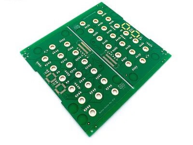
High voltage pcb is circuit board that can withstand high voltages and are commonly used in high-voltage electronic equipment. It must not only be able to withstand high voltages, but must also have excellent insulation properties and high temperature resistance, so as to ensure that no failure or damage occurs in the high-voltage operating environment.
Usually, high voltage pcb is made of materials with excellent insulating properties, such as glass fibre cloth covered copper foil board, PTFE board, polyimide board, etc. These materials not only have excellent insulating properties, but also have excellent temperature resistance. These materials not only have excellent insulating properties, but also can withstand high temperatures, resist corrosion, and have better durability.
High voltage pcb is mainly used in high voltage electronic equipment. For example:
- High-voltage discharge lamps: High voltage pcb is used to withstand the high-voltage current of the lamp;
- X-ray generator: high-voltage pcb is used to withstand the high voltage of the X-ray tube;
- electron beam welding machine: high-voltage pcb is used to withstand the high voltage of high-frequency electron beams;
- Inductor power supply: high voltage pcb is used to withstand the high voltage of inductors.
PCB layout and wiring design
Spacing control: In the high voltage PCB layout, maintaining sufficient electrical spacing is the key to ensure insulation performance. Between conductors of different potentials, such as high-voltage lines and low-voltage lines, power supply and signal lines, etc., sufficient distance should be maintained to prevent electrical breakdown. The specific spacing requirements need to be determined according to the working voltage, environmental conditions and other factors. Generally speaking, the higher the working voltage, the greater the required electrical distance. For example, in the high-voltage environment of 10kV, the minimum electrical distance between the conductors may need to reach several millimetres or even greater. At the same time, to avoid the formation of sharp corners or tips between the conductor, because these parts are prone to produce electric field concentration, reduce insulation performance, should try to use a smooth rounded transition.
Layering and shielding: Reasonable layering design helps to optimise the insulation performance of high voltage PCB. High-voltage circuits and low-voltage circuits are arranged in different layers, which can reduce electromagnetic interference and electrical coupling between layers. For the key high-voltage circuit layer, the grounding layer can be set up on both sides of the upper and lower sides of the shielding to reduce the impact of electric fields on other circuits. In addition, for some sensitive signal lines, similar shielding measures can also be used to prevent interference from high-voltage electric fields. For example, in the multi-layer PCB, the high-voltage power supply layer and the signal layer set up between the special isolation layer, and through the over-hole will be connected to the grounding of the layers together to form a good shielding effect.
High voltage pcb design principles:
- According to the circuit function unit custom PCB size and shape
In the initial stages of design, it is critical to have an in-depth understanding of the functional requirements of the circuit. Based on these requirements, we will accurately determine the size and shape of the PCB. In addition, in order to ensure that the PCB can perfectly fit the requirements of all functional units, we will carefully plan the layout of the space on the PCB, and strive to avoid over-densification of components while not causing any waste of space. - Follow the circuit layout principles, accurate positioning of special components
In circuit design, the placement of certain components (such as sensitive components, high-power components, etc.) need to be particularly careful. The performance and stability of these components have a significant impact on the overall circuit. Therefore, during the layout process, we will strictly follow the circuit layout principles to select the most suitable location for these special components. - Layout around the core components of the functional circuit and optimise the signal flow path.
In order to improve signal quality and effectively suppress interference and noise, the layout design should focus on the core components of each functional circuit. At the same time, should be committed to maintaining the consistency of the signal flow, in order to simplify the signal transmission path, reduce signal loss in the transmission process. - Component layout should follow the principle of uniformity, neatness and compactness, and optimise the leads and connections.
In the layout process, the components should be evenly, neatly and compactly arranged on the PCB, aiming to achieve the minimum use of space, and facilitate subsequent identification and maintenance work. In addition, it is also necessary to minimise and shorten the lead wires and connections between components, in order to reduce the complexity of the circuit design, reduce signal delay and the risk of potential interference. - Board edge component layout specifications to ensure stability and portability
In order to ensure the stability of the board and easy maintenance, components located at the edge of the board should be kept at least 2mm away from the edge. Circuit boards are usually designed as a rectangle, its aspect ratio is set to 3:2 or 4:3, such a design is easy to transport and facilitate the use, while effectively reducing the space occupied by the circuit board to enhance its portability.
High voltage PCB design needs to take into account the characteristics of the material and the layout of the principle, from the details of control to the overall planning, to ensure that it is stable and reliable in the high-voltage environment, for the development of high-voltage electronic equipment to build a solid foundation.