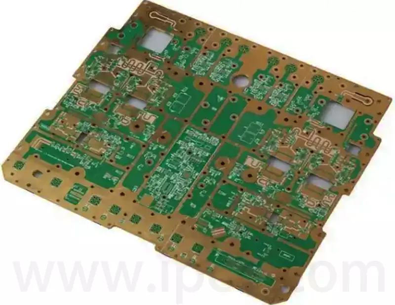
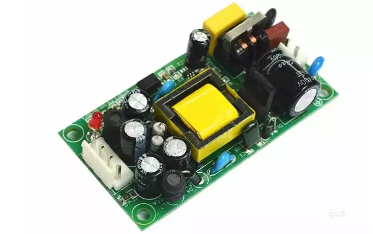
Energy harvesting pcb (Printed Circuit Board) is a circuit board applied in energy storage devices (e.g. batteries, supercapacitors) to manage, protect and control the charging and discharging process of the energy storage system.
Energy Harvesting PCB Advantages.
The high degree of integration enables it to be directly embedded in the motherboard of electronic devices, effectively saving space and promoting the development of miniaturisation and lightweight equipment. For example, in the smartphone sector, PCBs can replace traditional standalone battery cells, increasing battery capacity without significantly increasing size.
With good customisation capability, the shape, size and energy storage capacity can be flexibly adjusted according to the needs of different devices to suit various application scenarios.
Energy harvesting pcb manufacturing process is more mature, relying on existing PCB production technology and equipment, with large-scale production capacity, can effectively reduce manufacturing costs.
At present, the standard for energy harvesting pcb mainly includes the following aspects:
- Safety standards: energy harvesting pcb needs to meet the relevant safety standards to ensure its safety in normal use and in case of accidents. This includes the circuit board materials, insulation properties, flame retardant properties and other requirements.
- Interface standards: energy harvesting pcb needs to be a good interface with the energy storage equipment with four, to ensure that the circuit board can be normal communication and collaboration with the energy storage system. Interface standards include electrical interfaces, communication protocols.
- Charge and discharge management standards: energy harvesting pcb needs to have charge and discharge management functions, including current and voltage control, battery protection, battery equalisation and other aspects. The corresponding standards require that the board can be stable and efficient management and control of the charging and discharging process of the energy storage system.
- Environmental standards: energy harvesting pcb needs to comply with environmental protection requirements in the manufacturing and use process, including lead-free manufacturing, energy saving, resource recycling and other aspects of the requirements. At the same time, the waste disposal of circuit boards also needs to comply with relevant environmental standards.
For the standards of energy harvesting pcb, the specific requirements and specifications may vary from country to country, region to region and industry to industry. Therefore, when designing and manufacturing energy storage PCBs, it is necessary to refer to and comply with applicable standards to ensure product performance, safety and reliability. Meanwhile, research institutes, industry associations and relevant standardisation organisations are constantly promoting the development and updating of relevant standards to meet the needs of the development and application of energy storage technology.
Key considerations for energy harvesting pcb layout include the following:
Heat Management
Energy storage devices generate a large amount of heat during operation, and if the heat cannot be dispersed in a timely manner, it may lead to a decline in equipment performance or even damage. Therefore, PCB layout needs to reasonably plan the distribution of heat and adopt a scientific layout scheme to ensure that the heat can be quickly and effectively dispersed. For example, heat generating components and heat dissipation components can be closely arranged to reduce thermal resistance and improve the heat dissipation effect.
Electromagnetic compatibility (EMC)
The energy harvesting pcb is not only susceptible to external electromagnetic interference during operation, but also generates electromagnetic noise itself. In order to ensure the normal and stable operation of the equipment, the layout design needs to pay attention to electromagnetic compatibility. Specific measures include reasonable placement of high-frequency components, take shielding means, and good grounding to reduce electromagnetic interference.
Power and ground design
Power supply and ground is a crucial part of the energy harvesting pcb, and its layout is directly related to the performance and stability of the circuit. In the layout, it should be ensured that the power and ground lines have sufficient width to reduce line resistance and reduce power supply noise, while avoiding crossing with other signal lines to mitigate the impact of electromagnetic interference.
Signal Integrity Guarantee
In order to ensure the integrity of signal transmission and prevent signal distortion, PCB layout should try to shorten the length of signal lines and avoid parallel laying of signal lines with power and ground lines, thus reducing the impact of parasitic capacitance and parasitic inductance. In addition, the use of differential signal transmission can effectively enhance the anti-interference capability of the signal.
Anti-vibration design
Energy storage equipment may be affected by vibration in the actual use of the process, therefore, the PCB layout needs to consider the use of flexible materials, adjust the line spacing, improve the line’s anti-vibration ability, so as to enhance the stability and reliability of the overall circuit.
What are the difficulties in manufacturing energy harvesting pcb?
Because of the impact of high current, generally need to use thick copper plate, and thick copper plate in the manufacturing process will appear such as the following processing difficulties.
- Etching difficulties
Because of the increase in copper thickness, water exchange difficulty, in order to minimise the amount of water exchange caused by the side of the large amount of etching, the need for multiple rapid etching, with the side of the increase in the amount of etching, but also need to increase the etching compensation coefficient of the way to make up for the side of the etching. - Lamination difficulties
With the increase in copper thickness, the line gap is deeper, the amount of resin filling needs to be increased; due to the need to use the resin to fill the line gap and other parts of the maximum, with a high content of glue, resin mobility is good semi-cured sheet is to do the first choice for the thick copper plate. However, the increase in the use of semi-cured sheet will also increase the risk of sliding board, commonly used to increase the rivet method to strengthen the degree of fixation between the core plate. - Drilling difficulties
Thick copper boards are usually thicker than 2.0mm, in the drilling, X-RAY with the increase in copper thickness of the energy gradually attenuate, its penetration capacity will reach the upper limit. There will also be the problem of pad cracking when drilling PCBs. The traditional improvement method is to increase the pad, increase the peeling strength of the material, reduce the speed of the drilling of the falling knife and so on.
As a core component in the energy storage system, the energy harvesting pcb plays an important role in modern electronic devices by virtue of its high integration, good customisation and mature manufacturing process. However, its design layout needs to comprehensively consider various factors such as thermal management, electromagnetic compatibility, power and ground layout, signal integrity and anti-vibration performance to ensure system stability and reliability. At the same time, the difficulties of etching, laminating and drilling processes during the manufacturing of thick copper plates also put forward higher requirements for production technology.