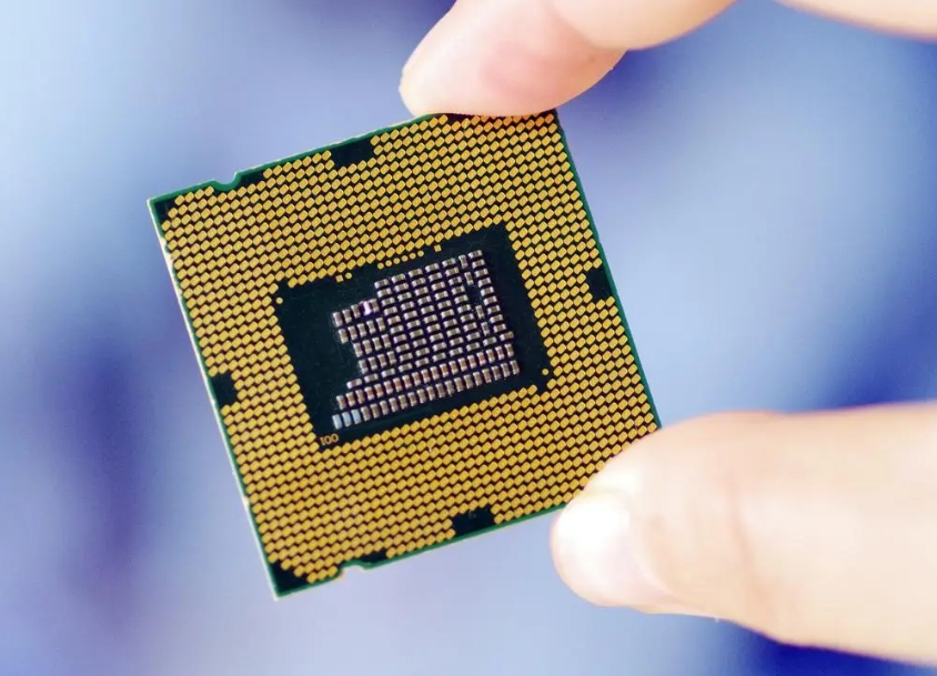
HDI circuit boards are highly integrated printed circuit boards with high density, miniaturization, and light weight, which can significantly improve the performance and functional density of electronic products. HDI board design specifications usually cover the following aspects:
Number of Layers and Thickness: HDI circuit boards usually use a multi-layer structure to accommodate more signal and power layers, with the number of layers often exceeding 8, and board thicknesses ranging from 0.3 mm to 1.6 mm.
Microvia and blind vias technology: Microvias and blind vias are widely used for inter-component connections, with microvia sizes generally less than 0.1 mm, and blind vias needing to be strictly controlled in terms of location and depth to ensure signal transmission efficiency.
High-precision layout design: Due to the density of components, the layout must be extremely accurate to safeguard electrical performance and thermal management effects, while preventing signal interference and maintaining signal integrity.
Material selection: High-performance substrate materials, such as those suitable for high-frequency signals or those with low dielectric constants, are preferred to ensure excellent electrical performance and heat dissipation.
Thermal solution: In view of the integration of more components, the thermal design becomes very critical, through the reasonable configuration of heat sinks and increase the heat dissipation layer and other measures to achieve effective heat dissipation.
Compliance with IPC standards: The design process needs to comply with the relevant IPC standards to ensure the reliability of the product during the manufacturing and use stages.
Layout principles for HDI circuit boards
With the continuous advancement of processing technology, such as the continuous reduction of PCB line width and aperture aperture, as well as the application of buried blind vias, microvia technology, pad vias, and HDI process, the network density per unit area of PCB is significantly increased. At the same time, EDA tools in the layout and routing methods are constantly optimized to adapt to the development of these advanced processes.
Layout design is an important part of PCB design, which requires comprehensive consideration of factors such as the division of circuit function modules, the path of critical signals and wiring rate. The following are the basic principles of HDI circuit boards layout:
In the layout, digital and analog circuits should be separated, and devices should be arranged as closely as possible. Wiring should avoid signals from digital circuits crossing the analog circuit area, and signals from analog circuits should avoid crossing the digital area to ensure that adequate isolation distance is maintained between the two areas.
- RF layout principles
Principle of physical partition: The RF transmitter part and receiver part are arranged separately, aiming at keeping the transmitter power amplifier away from the low-noise receiver amplifier and reducing mutual interference.
The principle of shortest RF signal line: RF system is usually a link structure, should be as short as possible to shorten the signal path of the corresponding link in the same area, while letting the input end of the link away from the output end. It is better to centralize the equipment on the same side to avoid the impedance discontinuity caused by over-hole.
Antenna Layout: The antenna part shall ensure that the feed line length is as short as possible and the feed point is close to the matching network, otherwise it will affect the antenna’s transmitting and receiving performance.
- Baseband layout principles
High-frequency high-speed circuits and sensitive circuits should be laid out as compactly as possible, and the sensitive signal circuit should be minimized. High-frequency high-speed circuits and sensitive circuits should be kept isolated to reduce interference. Specific sensitive parts include analog baseband I/Q signal lines, audio signals and clock signals, while the source of interference is mainly high-speed digital buses such as the SBI bus, whose digital signals are broad-spectrum and high-energy, and are prone to interference.
Power supply locations, such as battery contacts, should be close to major energy-consuming components, such as power amplifiers (PAs). The power supply network layout is recommended to be star-shaped, and decoupling capacitors should be placed in effective locations close to the loads.
Electrostatic protection devices (ESD) in the baseband section should be installed at the electrostatic inlet location, and wiring should be prioritized to ensure ESD protection before connecting to the inside of the chip.
When designing HDI circuit boards, there are several key factors that need to be addressed to ensure board performance, reliability and manufacturability.
The number of layers is critical; HDI circuit boards are usually multi-layer in structure, and the design needs to rationalize the location of the signal, ground, and power layers to ensure signal integrity and power stability. When designing, consider the signal transmission delay between different layers and avoid long distance signal alignment to reduce signal attenuation and interference.
Cabling density is a distinguishing feature of HDI. Designers should ensure proper line width and line spacing to achieve high-density lines in limited space. Use microvias and techniques such as blind and buried vias to increase the area that can be routed and to utilize space efficiently. Control line width and line spacing: Line width and line spacing are important factors affecting circuit board performance. When designing, it is important to set the line width and line spacing reasonably according to the actual application scenarios and signal transmission requirements of the circuit board.
Thermal management is also an important consideration. High-power components may lead to localized overheating, so reasonable space for heat dissipation should be left in the design, and the use of high thermal conductivity materials or heat sinks should be considered to improve thermal conduction. The design of power and ground lines is critical to the stability and reliability of the board. It is important to ensure that the power supply and ground layout is reasonable to reduce noise interference and improve the overall performance of the board.
Material Selection Considerations
Substrate material: the substrate material is the basis of the circuit board, and its performance directly affects the overall performance of the circuit board. In the selection of substrate materials, to consider its electrical properties, mechanical properties, thermal stability and other factors to ensure that the selected material meets the design requirements.
Conductive materials: conductive materials are key components of the circuit board, its conductivity and stability of the circuit board has an important impact on performance. To select conductive properties, good stability of conductive materials to ensure that the signal transmission quality and reliability of the circuit board.
Soldermask ink: Soldermask ink is used to protect the non-conductive parts of the circuit board to prevent short circuits and leakage. When selecting soldermask ink, it is important to consider its corrosion resistance, temperature resistance and adhesion and other factors to ensure that the circuit board in harsh environments can still maintain stable performance.
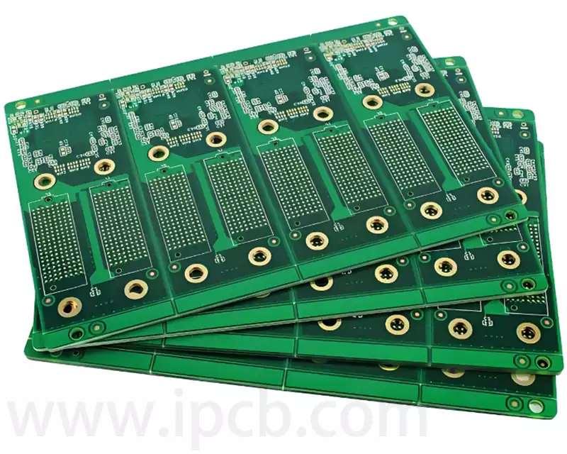
HDI third-order circuit board design and manufacturing process
Design Requirements Evaluation: First, according to the project requirements to determine the size of the circuit board, the number of layers and layout specifications, analyze the circuit characteristics, planning for the signal layer and power layer layout, as well as the need to use the impedance control, blind buried holes and other special features.
Schematic drawing: draw the circuit schematic according to the design requirements, select the appropriate components and complete the connection, and optimize the signal transmission path to reduce interference and signal loss.
Wiring planning: Design the wiring according to the schematic diagram to meet the needs of high-density interconnections, using fine lines and micro-hole technology.
Material selection strategy: Choose the right substrate material, such as FR-4 or high-frequency material, to ensure that the board performance meets the requirements. For third-order HDI circuit boards, thick copper foil and thin film materials are usually selected.
Manufacturing Drawing: Based on the wiring design, drawings for manufacturing are produced, including information such as the lines of each layer, aperture specifications, and the order of layer stacking.
Substrate pre-treatment: Pre-treatment processes are performed on the substrate, such as cleaning and deburring, in preparation for subsequent processes.
Pattern Layer Production: Production of line patterns according to the manufacturing drawings, including signal layer, power layer and ground layer.
Component Soldering: Use techniques such as SMT or BGA to complete the component mounting and soldering process.
Layer Stacking Process: Pressing and stacking the produced layers of circuit boards in the order required by the design.
Hole Processing: Use laser or mechanical drilling to complete through-hole, blind hole and buried hole processing.
Inner Layer Circuit Processing: Produce inner layer circuits and openings for blind buried holes.
Impedance control: According to the design requirements, control the line impedance by means of technology to ensure the quality of signal transmission.
Testing and verification: comprehensive testing and quality inspection of the finished HDI third-order circuit boards.
Surface treatment: Gold-plating, tin spraying and other surface treatment of the circuit board to enhance conductivity and corrosion resistance.
Final Inspection and Packaging: Completion of the final quality inspection to confirm compliance with the standards for packaging and shipment.
HDI board design and manufacturing is a systematic and complex project, through reasonable design principles and advanced manufacturing processes, HDI circuit boards can achieve high density, high performance and excellent thermal management, to meet the needs of modern electronic products for miniaturization and high integration.