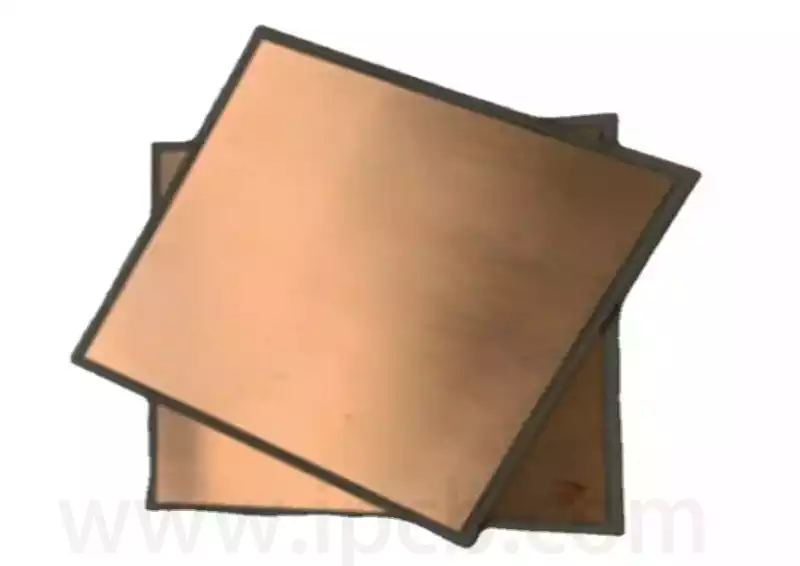
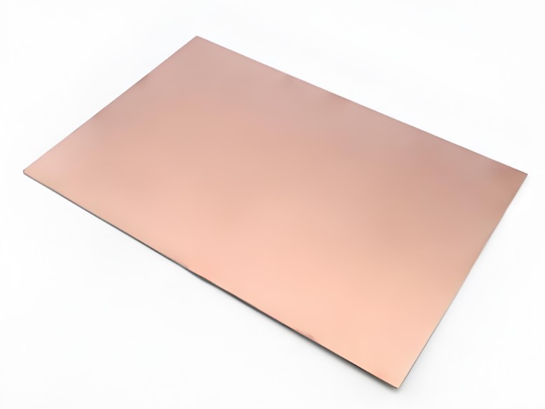
Ceramic substrate in accordance with the process points there are many kinds of, in addition to direct bonding copper (DBC) method, direct copper plating (DPC) method, laser activated metal (LAM) method, low-temperature co-fired ceramics (LTCC), high-temperature co-fired ceramics (HTCC) in addition to the AMB method of the technology that currently attracts much attention, that is, the active metal brazing technology.
Active Metal Brazing (AMB) is a further development of the DBC process technology, the working principle is: in the brazing electronic paste to add a small amount of active elements (Ti, Zr, V, Cr, etc.), using screen printing technology to print on the ceramic substrate, which is covered with oxygen-free copper and then put into a vacuum brazing furnace for sintering, and then etch out the graphics to produce circuits, and finally on the surface of the graphics of the chemical plating.
AMB (Active Metal Brazing, active metal brazing) process is a further development of the DBC process technology, it is the use of brazing material contains a small amount of active elements Ti, Zr and ceramic reaction to generate can be liquid brazing material wetting reaction layer, so as to achieve the ceramic-metal bonding of a method. AMB substrates rely on the chemical reaction between ceramic and active metal solder paste at high temperatures to achieve bonding, so its bonding strength is higher, better reliability, so the process is more suitable for the preparation of electric vehicles, power locomotives with IGBT module packaging ceramic copper-clad substrates.
AMB copper clad ceramic substrates generally use silver-copper-titanium solder pads or printed solder paste, but both methods have certain limitations:
① Solder pads used in the process of silver-copper-titanium solder pads are prone to oxidation and segregation of the active element Ti in the preparation process, resulting in a very low rate of formation of the material, the performance of the welded joints is poor.
② For the solder paste process, a large amount of organic matter volatilised when heated in a high vacuum, resulting in the brazing interface is not dense, there are more voids, making the substrate prone to high-pressure breakdown and crack-inducing problems in the service process.
The organic volatiles released will cause pollution and affect the service life.
When using silver-copper-titanium active brazing material to prepare AMB copper clad ceramic substrates, there are several main reasons for interface voids:
① Raw material surface quality: scratches, pits, oxidation, and organic contamination problems on the surface of ceramics and oxygen-free copper before soldering can negatively affect the wetting and spreading of the solder, which poses a potential risk of voids at the brazing interface.
② Solder printing quality: large-area solder paste printing process, more likely to solder paste leakage, uneven printing problems, solder melting once not spread to cover these leakage areas, will directly lead to the formation of voids.
③ Active element inactivation: AgCuTi solder paste in the active element Ti is very sensitive to oxygen, high-temperature brazing process, often require a vacuum better than 10-3Pa, if the vacuum can not meet the welding requirements leading to Ti oxidation inactivation, the solder can not wet the ceramic surface, resulting in large-area soldering, leakage phenomena such as welding.
④ Aolder paste volatile gas: brazing process, solder paste volatile gas will be flux package to form bubbles, in addition to the flux in the organic acid and metal oxide reaction will also produce bubbles, with the reaction of the bubbles gradually become larger, discharged bubbles will be in the surface of the solder paste to leave a dense air holes, and not discharged bubbles will be the same with the process of melting and solidification of the solder will be stagnant in the brazing interface, the formation of cavities.
⑤ Brazing process parameters: Ag-Cu-Ti active brazing material is often more than 800 ℃ in order to wet the surface of Si3N4, if the brazing temperature is too low or the holding time is too short, it will make Ti and ceramic surface reaction is not enough, resulting in brazing material can not completely wet the ceramic surface.
AMB silicon nitride copper-clad substrate preparation process, in terms of cavity rate control, high vacuum or high vacuum + inert gas brazing environment, pre-grease brazing process, appropriate brazing pressure, raw material cleaning (ceramic and copper sheet oil removal and de-oxidation treatment) can reduce the brazing interface cavity rate.

What is the relationship between AMB copper clad ceramic substrates and IGBT modules?
IGBT module is composed of chip, ceramic copper-clad board (circuit board), backplane, shell, and terminals. Its structural characteristics are mainly power semiconductor chip integrated in the ceramic copper-clad plate, through the lead bonding technology, to achieve the circuit interconnection between the chip, ceramic copper-clad plate, terminals. Currently high power modules on the heat dissipation requirements are increasingly high, using direct copper cladding method of preparation, heat dissipation capacity is limited, through the active metal brazing AMB process in a vacuum or inert gas to achieve bonding.
Development Prospects of AMB copper clad ceramic substrates
A series of encouraging policies and measures have been introduced in the context of governments around the world strongly supporting the development of strategic emerging industries such as new energy vehicles, 5G communications, and rail transport. These industries are the main application areas of AMB ceramic copper-clad laminates, and the policy support will indirectly drive the development of the AMB ceramic copper-clad laminates market. However, the AMB ceramic copper-clad laminate industry is also facing some challenges, such as the high cost of raw materials, complex production process, domestic enterprises still need to make further breakthroughs in the core technology (such as solder, process parameters, etc.), while at the same time also driving the domestic ultrasonic scanning microscope market demand.
As a further development of the direct bonded copper (DBC) process, the active metal brazing (AMB) technology achieves a strong bond between ceramic substrate and metal by introducing active elements, which is especially suitable for IGBT module packaging for electric vehicles and power locomotives. Its excellent bond strength and reliability make it a key material for IGBT module packaging against the backdrop of increasing demand for high-power heat dissipation.
Despite the promising future of AMB technology, it currently faces challenges in the preparation process, such as the tendency of solder wafers to oxidise and segregate reactive elements, and the volatilisation of organic substances from solder paste at high temperatures leading to interfacial voids. These problems may cause high-voltage breakdown, cracks, and shortened service life. In the future, by optimising the surface quality of raw materials, solder printing process, controlling the deactivation of active elements, reducing the volatility of solder paste gas and precisely regulating brazing process parameters, the interfacial voiding rate can be effectively reduced, which will further enhance the performance and reliability of AMB copper clad ceramic substrates.


