A peelable solder mask PCB is a printed circuit board with a peelable solder mask (temporary solder resist) that protects certain areas during surface preparation or assembly. That is, sometimes a printed circuit board needs to have selected areas of the board protected from solder flow onto contacts, terminals and plated through holes (PTH) during surface preparation or assembly.
Solder mask is a kind of protective film covering the surface of circuit boards, which can play the role of protecting circuit boards. During the manufacturing process of circuit boards, they are easily affected by the external environment, such as humidity, dust, etc., which can adversely affect the quality of circuit boards. The circuit board adhesive barrier film can effectively prevent the impact of these external factors on the circuit board, thus protecting the quality of the peelable solder mask pcb.
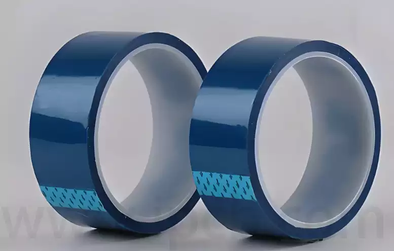
Common colours of blue adhesive: blue, also green, red
Covering method: coated in the designated area of the PCB by silk screen printing
Curing method: heat curing or UV curing
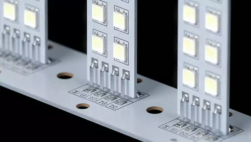
Stage of use: to protect the pads, holes, etc., before the completion of PCB soldering
Common uses:
Protect gold fingers, via holes, test points
Temporary mask before secondary assembly
Avoid solder contamination during soldering
Peters -Brand of the mask
Properties and Types of peelable solder mask
Peelable solder mask typically consists of thin film coatings with a thickness of 0.03 to 0.10 mm. These coatings are formulated from a variety of polymeric materials including acrylics, silicones, polyurethanes or epoxies. These polymers have selective adhesion properties that enable them to adhere to copper surfaces and FR-4 substrates used in PCBs. This property allows the soldermask to be peeled off the copper pads while still firmly adhering to the PCB substrate.
The peelable solder mask should be easy to peel from the copper surface and maintain strong adhesion to the FR-4 substrate, and should not leave any residue or contamination on the PCB after peeling. A slight change in the colour of the copper layer after peeling off the soldermask may indicate a poor surface finish on the printed board. In addition, the adhesion of soldermask is closely related to its thickness at high temperatures.
Based on material type, the peelable solder mask market is segmented into liquid photoimaging and dry film. The liquid photoimaging segment held the largest market share in 2023 and is expected to continue dominating the market throughout the forecast period. The growth of the segment is attributed to the growing demand for high density PCBs in various electronic devices. Liquid photoimaging soldermasks offer excellent printability and resolution for fine pitch and complex PCB designs, and have good adhesion to copper and other substrates to ensure reliable performance in harsh environments. The dry film segment is expected to grow at a significant CAGR during the forecast period. Dry film soldermasks are pre-coated onto a carrier film and then laminated onto PCBs, a process that provides precise and consistent application, making them suitable for high-volume production.
PCB bluing is a process that plays an important role in PCB production. It consists of applying the blue adhesive to specific parts of the PCB, mainly through screen printing or screen printing on aluminium sheets. The blue glue can prevent solder paste bridging adjacent pads to avoid short circuits, protect non-soldered areas of copper foil against oxidation and corrosion, and can also be fixed for small components and marking. After coating, the adhesive is baked and cured to turn it from a liquid to a solid state for firm adhesion. After completion of the soldering process, the blue adhesive that is not covered by the solder is removed to reveal the copper foil that needs to be processed later. The process parameters are strict, with different requirements for different situations, and are critical to PCB quality and performance.
The role of the blue glue
- Protective effect: blue glue can prevent solder paste in the welding process to bridge the adjacent pads to avoid short-circuit phenomenon. At the same time, covered in non-welded areas of the copper foil, can prevent air, moisture and other oxidation corrosion of copper foil, effectively extend the service life of the PCB.
- Aesthetics and labelling: It gives the PCB a uniform and clear visual effect and facilitates the identification of component layout and alignment. In addition, it can also be used as a temporary marking, which is convenient for process identification and quality control in the production process.
As an indispensable temporary protective layer in the manufacture of printed circuit boards (PCBs), peelable solder mask plays a vital role in the surface treatment and assembly process. It not only effectively protects sensitive areas from solder contamination and avoids short circuits, but also extends the life of the PCB in harsh environments.
Coated by means of screen printing or aluminium screen printing, and cured by heat or UV curing, this ‘blue glue’ provides a solid guarantee for the quality and performance of PCBs. The market for peelable solder mask will continue to grow strongly as the demand for high-density PCBs for electronic devices continues to grow. The two main types, liquid photoimaging and dry film, each have their own advantages and together they fulfil the market’s need for precise, efficient and reliable protection. In particular, the rapid growth in automotive electronics, consumer electronics and industrial applications is further fuelling the widespread use of peelable soldermask for lead-free soldering and more sustainable manufacturing practices.