As a core component of electronic devices, the performance stability of RF circuit boards directly affects the overall operational effectiveness of the device. However, in complex electromagnetic environments, RF circuit boards are highly susceptible to various forms of electromagnetic interference, which can lead to performance degradation or even failure. Therefore, implementing effective shielding measures to protect RF circuit boards is of utmost importance. This article will provide a detailed overview of key design techniques for RF circuit boards in terms of layout, routing, and cavity treatment, with the aim of enhancing the circuit’s interference resistance and overall performance.
Design Techniques for RF Circuit Boards
RF Layout
The primary focus here is on the component placement layout for multi-layer boards. The key to component placement layout is to fix the position of components on the RF path, adjust their orientation to minimise the length of the RF path, and keep the input as far as possible from the output. High-power circuits and low-power circuits should be separated as much as possible, and sensitive analogue signals should be kept away from high-speed digital signals and RF signals.
The following techniques are commonly used in layout design.
- Straight-line layout
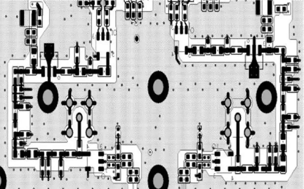
RF main signal components should preferably be arranged in a straight-line layout, as shown in Figure 1. However, due to PCB board and cavity space constraints, a straight-line layout is often not feasible. In such cases, an L-shaped layout can be used, but a U-shaped layout should be avoided whenever possible (as shown in Figure 2). If a U-shaped layout is unavoidable, the distance between the input and output should be maximised, preferably to at least 1.5 cm.
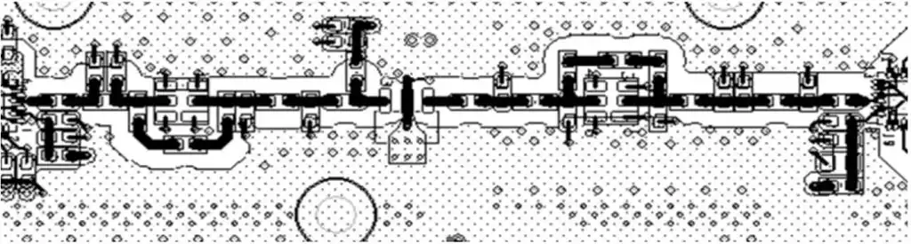
Additionally, when using an L-shaped or U-shaped layout, the turning point should not be immediately after entering the interface, as shown in Figure 3 (left), but rather after a short straight section, as shown in Figure 3 (right).
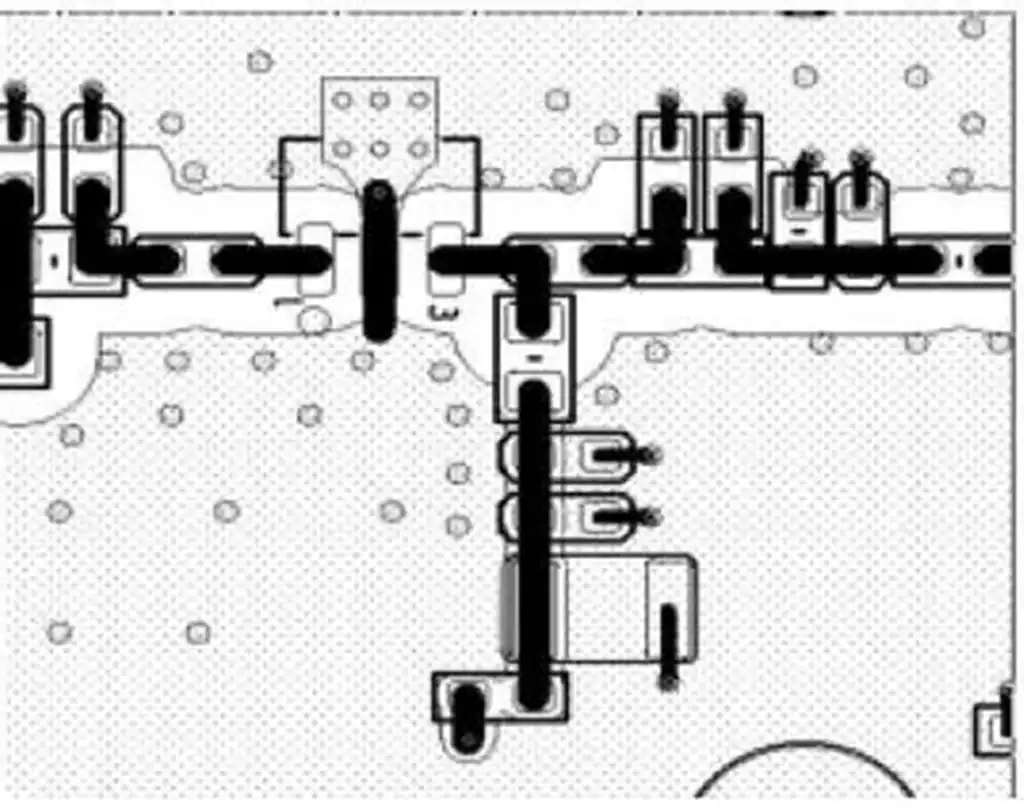
- Identical or Symmetrical Layout
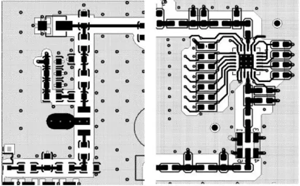
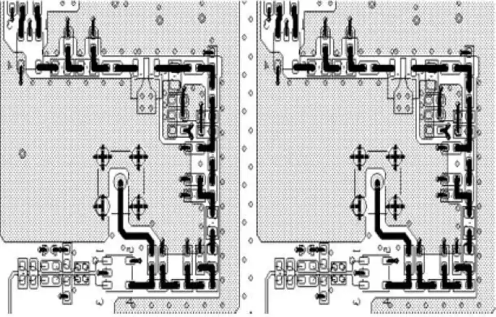
Identical modules should be designed with identical or symmetrical layouts whenever possible, as shown in Figures 4 and 5.
- Cross-shaped layout
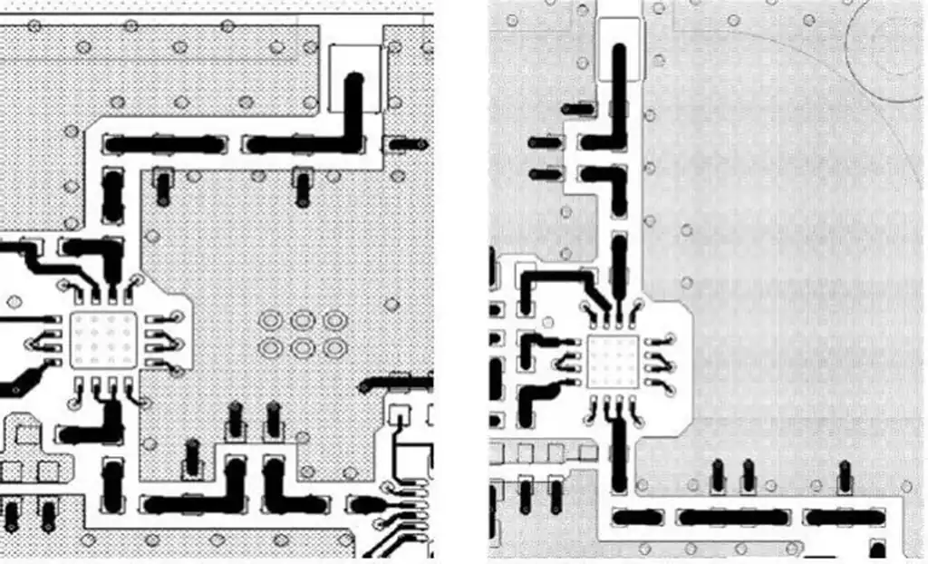
The feed inductance of the offset circuit is placed perpendicular to the RF channel, as shown in Figure 6, mainly to avoid mutual inductance between inductive components.
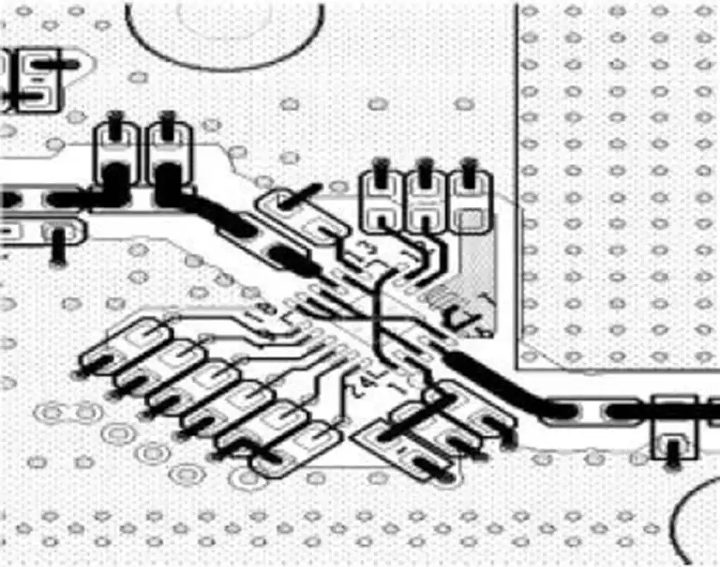
- 45-degree layout
To make reasonable use of space, components can be laid out at a 45-degree angle to minimise the length of RF lines, as shown in Figure 7.
RF Wiring
The general requirements for wiring are as follows: RF signal traces should be short and straight, minimise sudden changes in trace width, reduce the number of vias, avoid crossing with other signal traces, and add as many ground vias as possible around the RF signal traces.
The following are some commonly used optimisation methods:
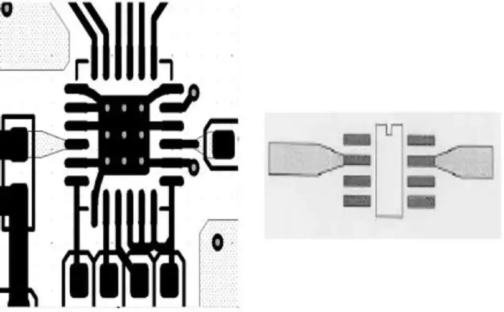
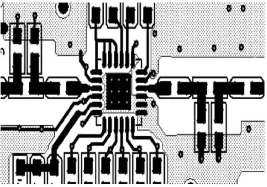
- Gradient line processing
When the width of the RF line is significantly larger than the width of the IC device pin, the line width in contact with the chip is processed using a gradient method, as shown in Figure 8.
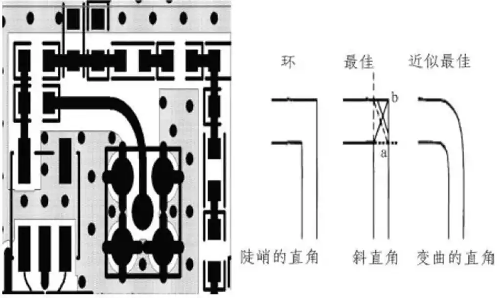
- Arc Line Treatment
When RF lines cannot be straight, arc line treatment is applied to reduce RF signal radiation to the outside and mutual coupling. Experimental evidence shows that using curved right angles at transmission line corners can maximise the reduction of return loss. As shown in Figure 9.
- Grounding and Power Supply
The grounding wire should be as thick as possible. Whenever possible, grounding should be applied to every layer of the PCB board, and the grounding should be connected to the main ground. Multiple grounding vias should be used to minimise grounding impedance.
For RF circuits, the power supply should avoid using planar segmentation. A solid power supply plane not only increases the radiation of RF signals from the power supply plane but also makes it more susceptible to interference from RF signals. Therefore, power lines or planes are typically designed in a long strip shape, with the width determined based on current requirements. They should be as wide as possible while maintaining sufficient current capacity, but should not be unnecessarily widened. When designing power lines, loops must be avoided.
Power lines and ground lines should be parallel to RF signal lines but should not overlap. At intersections, a perpendicular cross-over configuration is recommended.
- Cross-crossing treatment
RF signals and IF signals cross each other, and a ground plane should be placed between them whenever possible.
When RF signals cross other signal lines, a ground plane connected to the main ground should be placed along the RF signal line between them. If this is not possible, ensure that they cross each other at right angles. Other signal lines here also include powe.
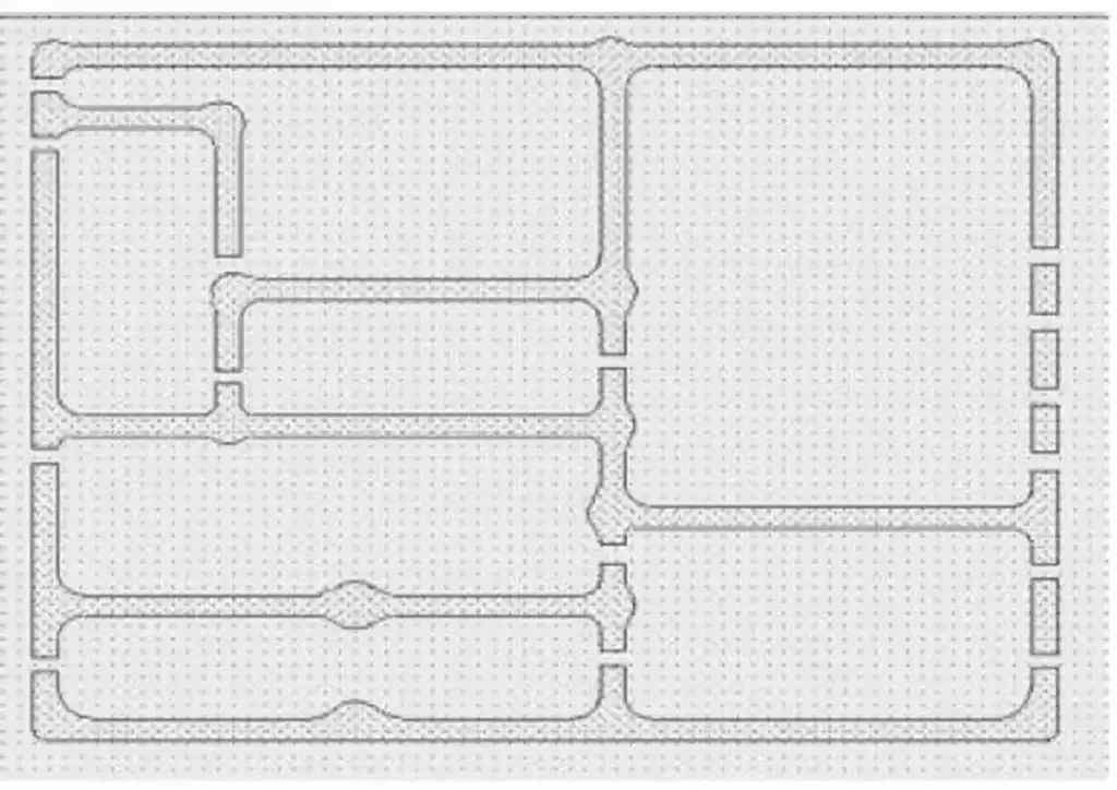
- Grounding Treatment
Grounding treatment is applied to radio frequency signals, interference sources, sensitive signals, and other important signals. This not only enhances the signal’s interference resistance but also reduces its interference with other signals. As shown in Figure 10.
- Copper Foil Processing
Copper foil processing must be smooth and flat, with no long lines or sharp corners. If sharp corners, narrow copper foil, or edges cannot be avoided, add several ground vias at these locations.
- Spacing Treatment
The RF line must be at least 3W wide from the edge of the adjacent ground plane, and there must be no non-grounded vias within 3W.
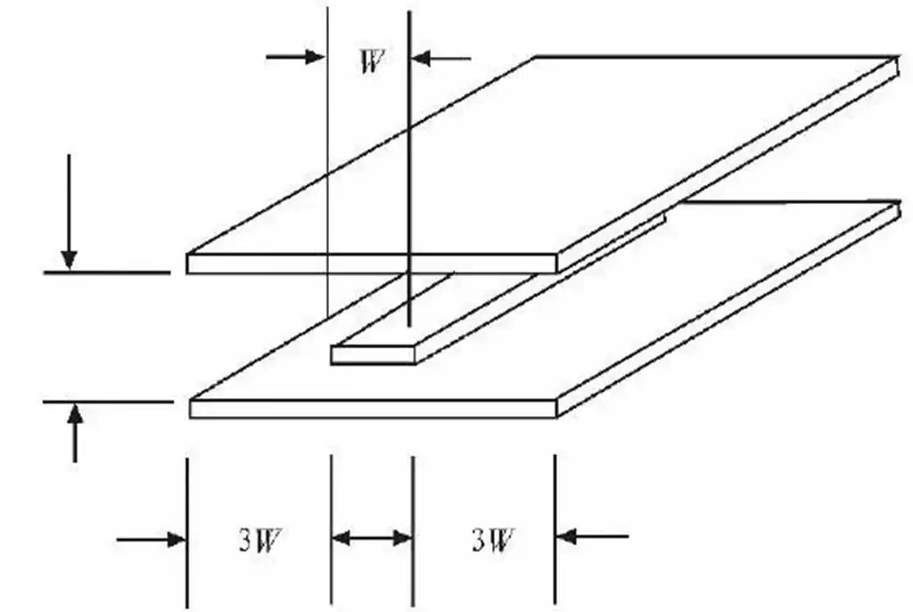
RF lines on the same layer should be shielded, and ground vias should be added to the ground plane. The spacing between vias should be less than 1/20 of the wavelength (λ) corresponding to the signal frequency, and they should be evenly spaced and neatly arranged. The edge of the shielding copper plane should be 2W wide or 3H high from the RF line, where H represents the total thickness of the adjacent dielectric layer.
Cavity Treatment
For the entire RF circuit, the RF units of different modules should be isolated using cavities, especially between sensitive circuits and strong radiation sources. In high-power multi-stage amplifiers, isolation between stages should also be ensured. After the entire circuit is properly arranged, the next step is to treat the shielded cavity. The following precautions should be observed when treating the shielded cavity:
The entire shielded cavity should be designed as a regular shape to facilitate moulding. Each shielded cavity should be designed as a rectangle, avoiding square-shaped shielded cavities.
The corners of the shielded cavity should be rounded. Shielded metal cavities are typically cast, and rounded corners facilitate demoulding during casting. As shown in Figure 12.
The perimeter of the shielded cavity is sealed. The interface lines entering the cavity typically use strip lines or microstrip lines, while the internal modules within the cavity use microstrip lines. The junctions between different cavities are treated with slots, with a slot width of 3 mm, and the microstrip lines are positioned exactly in the centre.
Metalised holes with a diameter of 3mm are placed at the corners of the cavity to secure the shielding housing. On longer cavities, an equal number of metalised holes are uniformly distributed to reinforce the structural integrity.
The cavity is typically designed with openings to facilitate welding of the shielding housing. The cavity wall is generally at least 2 mm thick, with two rows of openings for through-holes on the cavity surface. The through-holes are staggered, with a spacing of 150 mils between holes in the same row.
RF circuit board design is a complex system engineering task that requires meticulous design and optimisation across multiple stages, including layout, routing, and cavity processing. By following the above design techniques, designers can effectively reduce electromagnetic interference in the circuit, enhance the RF circuit’s interference resistance, and maximise overall performance. While practical experience and engineering design capabilities are crucial, drawing on others’ experiences and combining them with continuous exploration and reflection are key to achieving success in RF circuit board design.