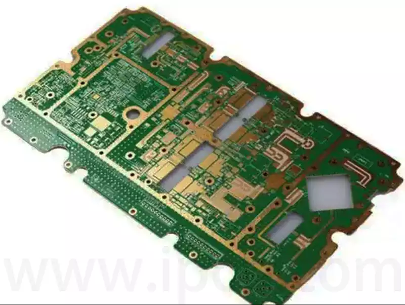
Electroplating via filling is a key technology in the field of modern high-density electronic packaging. It not only greatly enhances the design flexibility and performance of PCB boards, but also demonstrates significant advantages in product reliability, heat dissipation capabilities, and production efficiency. This article will explore the many advantages of electroplating via filling in depth and analyze the key physical parameters and substrate factors that affect its effectiveness, with the aim of providing a comprehensive perspective for understanding and optimizing this process.
Advantages of Electroplating Hole Filling Process
The electroplating hole filling process offers numerous significant advantages. Not only does it reduce the need for additional process development, but it is also highly compatible with existing process equipment, providing a strong guarantee for achieving excellent product reliability.
Significant Advantages of Electroplating Hole Filling
Supporting High-Density Design: This process facilitates the implementation of stacked holes and via-on-pad designs, significantly increasing the density of the substrate. This enables the use of more packaging substrates with I/O pins, aligning with the trend toward miniaturization and integration in electronic products.
Optimizing Electrical Performance: It helps improve electrical performance, providing strong support for high-frequency designs, enhancing connection reliability, increasing operating frequency while effectively avoiding electromagnetic interference, and ensuring stable operation of electronic devices in complex environments.
Enhancing Heat Dissipation: The electroplating via-filling process has a positive effect on heat dissipation, helping electronic devices better dissipate heat, reducing the risk of performance degradation and damage caused by overheating, and extending the service life of the equipment.
Completion of Critical Processes in a Single Step: Hole filling and electrical interconnection can be completed in a single step, avoiding defects that may arise from using resin or conductive adhesive for hole filling. It also eliminates inconsistencies in the coefficient of thermal expansion (CTE) caused by other materials, ensuring product quality stability.
Improved Circuit Design and Manufacturing Precision: Blind holes are filled with electroplated copper, avoiding surface凹陷 issues and facilitating more precise circuit design and manufacturing. Additionally, after electroplating, copper columns form inside the holes, which have superior conductivity compared to conductive resin/adhesive, further improving the heat dissipation performance of the pcb board.
Physical parameters requiring further study
In the electroplating hole-filling process, several physical parameters require in-depth study, including anode type, anode-cathode spacing, current density, agitation, temperature, rectifier, and waveform.
Anode type: Anodes are primarily divided into soluble anodes and insoluble anodes. Soluble anodes typically use phosphorus-containing copper balls, but they tend to produce anode sludge during use, which can contaminate the plating solution and impair its performance. Insoluble anodes, also known as inert anodes, are generally composed of titanium mesh coated with a mixture of tantalum and zirconium oxides. They offer advantages such as good stability, no need for anode maintenance, and no anode sludge generation, making them suitable for pulse or direct current electroplating. However, their additive consumption is relatively high.
Anode-Cathode Spacing: In electroplating hole-filling processes, the spacing between the cathode and anode is critically important, and design varies depending on the type of equipment. However, regardless of the design, it must adhere to Faraday’s Law.
Agitation: There are various agitation methods, including mechanical oscillation, electrical vibration, pneumatic vibration, air agitation, and jet (Eductor) agitation. For electroplating hole filling, it is generally preferred to add jet design to the traditional copper tank configuration. However, jet design involves multiple factors, such as whether to use bottom jets or side jets, the layout of jet nozzles and air agitation tubes within the tank, the jet flow rate per hour, the distance between jet nozzles and the cathode, the front-to-back position of side jets relative to the anode, whether bottom jets cause uneven agitation (stronger agitation at the bottom than at the top of the plating solution), the number, spacing, and angle of jets on the jet nozzles, etc. These factors must be thoroughly considered during copper tank design and tested extensively. Additionally, the most ideal approach is to install flow meters on each jet tube to monitor flow rates. Due to the high flow rates, the solution tends to heat up, making temperature control critical.
Current density and temperature: Low current density and low-temperature environments can reduce the deposition rate of surface copper while ensuring sufficient Cu²⁺ and brighteners enter the pores. Under such conditions, pore-filling capability is enhanced, but electroplating efficiency may decrease.
Rectifier: The rectifier is a critical component in the electroplating process. Currently, most research on electroplating hole filling is limited to full-plate electroplating. If patterned electroplating hole filling is considered, the cathode area becomes very small, imposing extremely high requirements on the rectifier’s output precision. The selection of rectifier output precision should be determined based on the product’s line width and via size; the finer the lines and smaller the holes, the higher the precision requirements for the rectifier, typically requiring an output precision of within 5%. However, selecting a rectifier with excessively high precision increases equipment investment. In terms of rectifier output cable wiring, the rectifier should be installed as close as possible to the plating tank to minimize output cable length and reduce pulse current rise time. Additionally, the selection of output cable specifications should ensure that the line voltage drop of the output cable is within 0.6V at 80% of the maximum output current. Generally, the required cable cross-sectional area is calculated based on a current-carrying capacity of 2.5A/mm². If the cable cross-sectional area is too small or the length is too long, it will result in excessive line voltage drop, preventing the output current from reaching the required production value. For plating tanks with a width greater than 1.6m, a dual-side power supply configuration should be considered, ensuring that the lengths of the dual-side cables are equal to control the current error between the two sides within a certain range. Additionally, each flying bar in the plating tank should be connected to a rectifier on both sides to allow separate adjustment of the current on each side.
Waveform: From a waveform perspective, electroplating hole filling primarily employs two methods: pulse electroplating and DC electroplating, both of which have been studied extensively. DC electroplating hole filling uses traditional rectifiers, which are easy to operate but ineffective for thicker workpieces. Pulse electroplating hole filling uses PPR rectifiers, which involve relatively more operational steps but have stronger processing capabilities for thicker in-process boards.
The Impact of Substrates on Electroplating Hole Filling
The impact of substrates on electroplating hole filling cannot be overlooked, primarily involving factors such as dielectric layer material, hole shape, aspect ratio, and chemical copper plating layer.
Dielectric Layer Material: The material of the dielectric layer can influence the effectiveness of hole filling. Compared to non-glass-reinforced materials, glass-fiber-reinforced materials present greater challenges in hole filling. In particular, glass-fiber protrusions within the holes can have adverse effects on chemical copper plating. In such cases, the key challenge in electroplating hole filling lies in enhancing the adhesion of the chemical plating seed layer, rather than the filling process itself. In fact, electroplating hole filling on glass-fiber-reinforced substrates has already been applied in actual production.
Aspect ratio: Currently, manufacturers and developers place great emphasis on hole filling technology for holes of various shapes and sizes. Hole filling capability is significantly influenced by the aspect ratio. Relatively speaking, DC systems are more widely adopted in commercial applications. In production, the size range of holes is typically narrow, with diameters generally between 80μm and 120μm, depths between 40μm and 80μm, and aspect ratios not exceeding 1:1.
Chemical copper plating layer: The thickness, uniformity, and post-plating dwell time of the chemical copper plating layer all influence hole-filling performance. If the chemical copper layer is too thin or uneven in thickness, it can result in poor hole-filling effectiveness. It is generally recommended to perform hole-filling when the chemical copper thickness exceeds 0.3μm. Additionally, oxidation of the chemical copper layer can have a negative impact on hole-filling effectiveness.
Electroplating hole-filling processes, through optimized design, enhanced performance, and improved reliability, have become an indispensable technology in modern high-density electronic packaging.