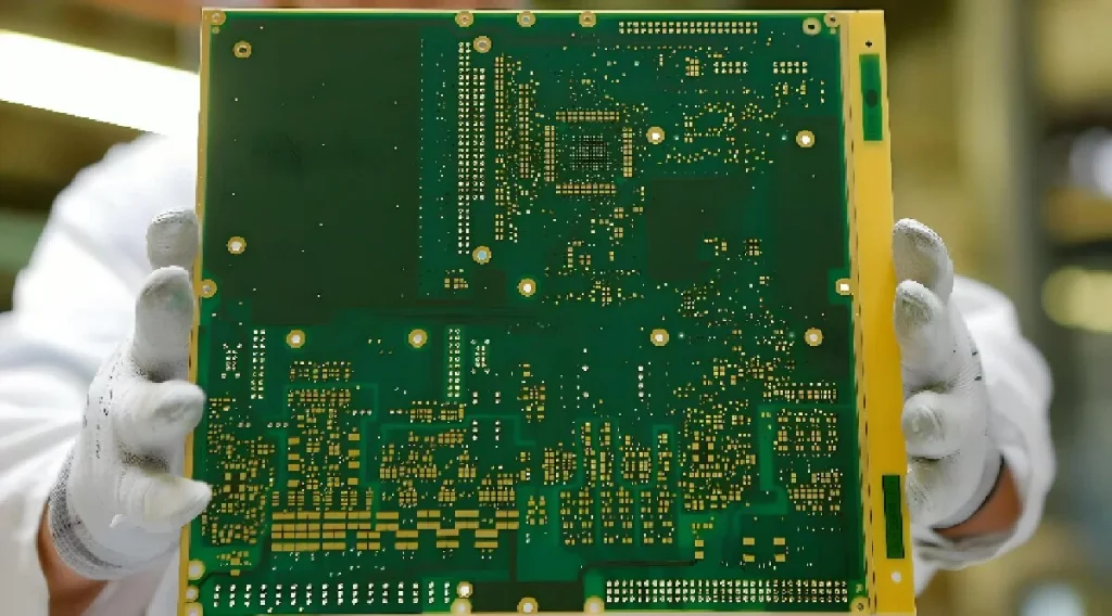
PCB chamfering, simply put, involves bevelling the edges of printed circuit boards. This process is typically carried out after the boards have been cut, using specialised chamfering machinery or hand tools to transform the board’s right-angled edges into bevelled surfaces at a specific angle. This treatment not only enhances the aesthetic appearance of the circuit board but, more importantly, improves the product’s safety and reliability.
Functions of PCB Chamfering
1.Protecting Circuit Board Edges
As circuit board edges are relatively fragile and susceptible to abrasion damage, chamfering provides protective benefits, making the edges less prone to damage.
2.Extended Service Life
Chamfered edges present a smoother profile. Without this treatment, sharp edges may cause finger lacerations during handling, compromising user experience. Furthermore, edge damage during operation can shorten the board’s lifespan. PCB chamfering prevents these issues, thereby prolonging the PCB’s service life.
PCB chamfering may impact signal quality as follows:
- Reduced signal reflection: Sharp 90-degree corners cause signal waves to reflect at the angle, inducing distortion and interference. Chamfering minimises reflection, improving signal integrity.
- Reduced signal crosstalk: Chamfering diminishes electromagnetic interaction between adjacent traces, mitigating crosstalk effects and supporting stable signal transmission.
Improved impedance matching: Chamfering promotes more uniform PCB impedance, enhancing signal matching and reducing transmission losses.
Reduced edge damage: Unchamfered sharp edges are susceptible to mechanical damage or wear, compromising signal quality and overall PCB reliability.
Enhanced high-frequency performance: For high-frequency signal transmission, chamfering minimises edge reflections and attenuation, preserving signal integrity at elevated frequencies.
Reduced Radiation Noise: Sharp 90-degree corners generate significant radiation noise, whereas chamfers mitigate this phenomenon.
In printed circuit board (PCB) design, the pcb chamfer angle of gold fingers and the thickness of the gold plating are critical factors in ensuring product reliability, yet these details are often overlooked by engineers. As the interface connecting the PCB to external devices, the design of gold fingers must balance mechanical protection with electrical conductivity. The chamfered structure prevents physical damage during insertion and removal, while an adequately thick gold plating layer guarantees excellent conductivity and wear resistance. The synergistic design of these two elements directly impacts the product’s lifespan and stability.
The pcb chamfer angle typically ranges between 30° and 45°, with the specific choice depending on the insertion method. For instance, vertical insertion interfaces (such as memory modules) often employ a 45° chamfer to achieve a smooth insertion experience and minimise plating scratches. Conversely, horizontal insertion interfaces (such as PCIe slots) benefit more from a 30° chamfer to lower contact pressure and minimise wear. Excessively large angles (e.g., exceeding 60°) reduce the effective contact area, increasing contact resistance; conversely, angles too small (e.g., below 20°) may create sharp edges that scratch contact points and cause current concentration at the edges during plating, leading to issues like excessive plating thickness or scorching. The selection of gold plating thickness must account for the operating environment and insertion/removal frequency. Industrial-grade equipment (such as server motherboards) typically requires a minimum plating thickness of 3μm to withstand over 5,000 insertion cycles; consumer electronics (such as mobile phone chargers) may appropriately reduce this to 1-2μm. However, it should be noted that thicker gold plating is not necessarily better. When exceeding 5μm, internal stresses may develop within the gold layer, leading to cracking or peeling of the plating and compromising the PCB’s flatness. Furthermore, the purity of the gold plating must correspond to its thickness. High-purity gold (99.99%) is suitable for thin coatings (1-2μm), while gold plating containing a small amount of nickel alloy (99.9%) is more appropriate for thicker coatings (3-5μm) to enhance wear resistance and adhesion.
The principle for matching chamfer angles with plating thickness is as follows: the pcb chamfer angle influences the distribution requirements for plating thickness. For gold fingers with a 45° chamfer, the plating thickness on the chamfered surface should exceed 80% of the base thickness. For instance, if the base has a 3μm gold plating, the chamfered surface must achieve at least 2.4μm to prevent oxidation or wear. For gold fingers with a 30° chamfer, due to the longer chamfered surface, the plating thickness should match the base surface. For instance, if the base surface has 3μm plating, the chamfered surface should also have 3μm to prevent accelerated localised plating wear.
In PCB design, the chamfer angle of gold fingers and the thickness of the gold plating are critical factors in ensuring product reliability, yet these details are often overlooked by engineers. As the interface connecting the PCB to external devices, the design of gold fingers must balance mechanical protection with electrical conductivity. The chamfered structure prevents physical damage during insertion and removal, while an adequately thick gold plating layer guarantees excellent conductivity and wear resistance. The synergistic design of these two elements directly impacts the product’s lifespan and stability.
The pcb chamfer angle typically ranges between 30° and 45°, with the specific choice depending on the insertion method. For instance, vertical insertion interfaces (such as memory modules) often employ a 45° chamfer to achieve a smooth insertion experience and minimise plating scratches. Conversely, horizontal insertion interfaces (such as PCIe slots) benefit more from a 30° chamfer to lower contact pressure and minimise wear. Excessively large angles (e.g., exceeding 60°) reduce the effective contact area, increasing contact resistance; conversely, angles too small (e.g., below 20°) may create sharp edges that scratch contact points and cause current concentration at the edges during plating, leading to issues like excessive plating thickness or scorching. The selection of gold plating thickness must account for the operating environment and insertion/removal frequency. Industrial-grade equipment (such as server motherboards) typically requires a minimum plating thickness of 3μm to withstand over 5,000 insertion cycles; consumer electronics (such as mobile phone chargers) may appropriately reduce this to 1-2μm. However, it should be noted that thicker gold plating is not necessarily better. When exceeding 5μm, internal stresses may develop within the gold layer, leading to cracking or peeling of the plating and compromising the PCB’s flatness. Furthermore, the purity of the gold plating must correspond to its thickness. High-purity gold (99.99%) is suitable for thin coatings (1-2μm), while gold plating containing a small amount of nickel alloy (99.9%) is more appropriate for thicker coatings (3-5μm) to enhance wear resistance and adhesion.
The principle for matching chamfer angles with plating thickness is as follows: the chamfer angle influences the distribution requirements for plating thickness. For gold fingers with a 45° chamfer, the plating thickness on the chamfered surface should exceed 80% of the base thickness. For instance, if the base has a 3μm gold plating, the chamfered surface must achieve at least 2.4μm to prevent oxidation or wear. For gold fingers with a 30° chamfer, due to the longer chamfered surface, the plating thickness should match the base surface. For instance, if the base surface has 3μm plating, the chamfered surface should also have 3μm to prevent accelerated localised plating wear.
Key Implementation Points for PCB Chamfering
When implementing PCB chamfering, the following points require attention:
- Choice of chamfer angle: The angle size should be determined based on the PCB’s thickness, material, and operating environment to ensure optimal structural strength and safety.
- Control of machining precision: Strict control of machining accuracy is required during the chamfering process to avoid unnecessary damage to the PCB.
- Quality control: Quality inspection should be conducted on each batch of PCB chamfering to ensure all products meet specified standards and requirements.