Component spacing design on PCBA represents a pivotal aspect of electronic product development, where precision directly influences circuit electrical performance, thermal efficiency, manufacturing feasibility, and the stable operation of the final product. Component spacing is not merely a matter of spatial allocation, but rather an art form that comprehensively considers electrical safety, thermodynamics, signal integrity, and production processes.
Electrical Safety Clearances: Preventing Arc Breakdown and Leakage Current
Electrical safety clearances aim to effectively prevent arc breakdown and leakage current phenomena. Their specific values require comprehensive consideration of operating voltage, environmental pollution levels, and the characteristics of the insulation materials used. International standards such as IPC-2221 and IEC 60950-1 provide explicit regulations for this.
- Clearance Requirements for Different Voltage Levels
Low-voltage circuits (0-30V): Minimum distance between conductors is 0.1 millimetres (4 mils), e.g., interconnects between CPU and memory on mobile phone motherboards.
Medium-voltage circuits (30–150V): Spacing is calculated using the formula: Spacing (mm) = 0.1 + V peak × 0.01. For instance, a 48V industrial power supply board requires a minimum spacing of 0.58 millimetres.
High-voltage circuits (>150V): Primary-side AC lines (e.g., L-N lines in switching power supplies) must maintain a minimum clearance of 2.5 millimetres. Clearance between primary and secondary sides requires a minimum of 6.4 millimetres. Additionally, isolation grooves beneath optocouplers should be incorporated to enhance insulation effectiveness.
- Compensation Measures for Extreme Environments
Special environments impose heightened requirements on electrical safety clearances:
High-altitude environments: For equipment operating above 2000 metres, the reduced air density diminishes insulation performance, necessitating a 1.48-fold increase in electrical clearances.
Salt-fog environments: In corrosive conditions such as salt spray, surface creepage distances must be increased by 300% through methods like applying triple-proof coating to prevent leakage caused by surface conductive pathways.
- Challenges in Integrated Circuit Pin Spacing
In QFP packages with 0.4mm pin pitch, pad widths measure just 0.2mm, with gaps also at 0.2mm. To address this extreme constraint, solder mask bridges must be applied between pads, alongside strict control of reflow soldering temperatures to prevent bridging during assembly. - Component Physical Spacing: Ensuring Manufacturing and Assembly
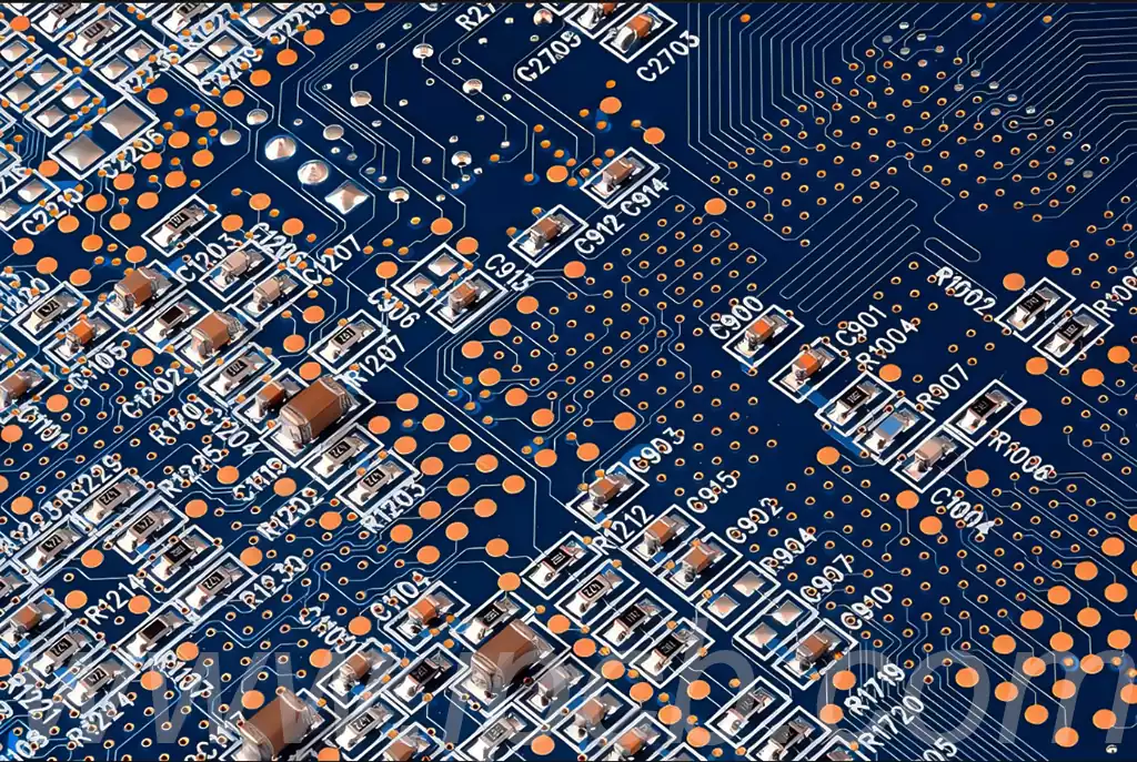
The actual physical spacing between components is crucial for ensuring smooth PCBA manufacturing and assembly. It impacts solder paste printing, component placement accuracy, soldering quality, and subsequent inspection. - Spacing Specifications for Surface Mount Devices (SMDs)
Same-type components: For instance, the minimum spacing between 0201-packaged resistors and capacitors should be greater than or equal to 0.3 millimetres to prevent solder paste adhesion during printing.
Disparate Components: Where adjacent components differ in height, the minimum spacing may be calculated using the formula 0.13H + 0.3 mm, where H represents the height difference between adjacent components. For instance, placing a 2-millimetre-high inductor beside a 3-millimetre-high electrolytic capacitor requires a minimum spacing of 0.43 millimetres.
Fine-pitch components: For integrated circuits with 0.5 mm pin pitch, pad widths are as narrow as 0.25 mm, necessitating laser-cut stencil technology for precise solder paste deposition.

- Spatial Constraints for Specialised Components
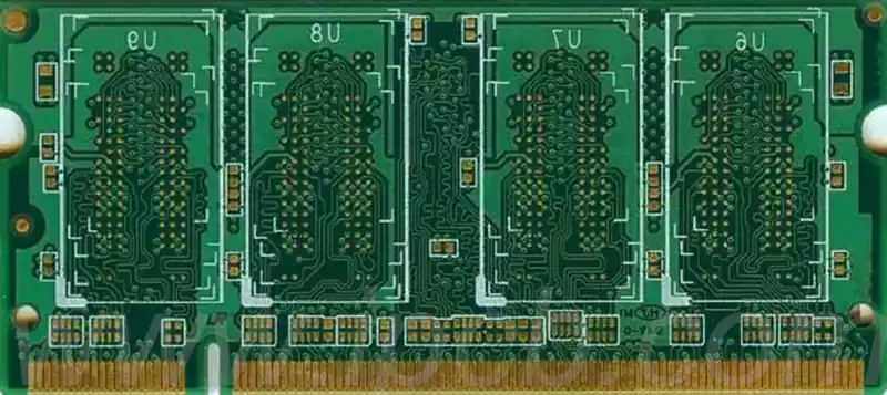
BGA packages: A 3–5 mm no-placement zone must typically be maintained around BGA packages. Additionally, no other BGA components may be placed within an 8-millimetre projection zone on the reverse side to prevent blind spots during X-ray inspection.
High-power components: The spacing between MOSFETs and heat sinks should exceed 2 millimetres. For effective thermal dissipation, copper foil should be laid out in teardrop-shaped heat dissipation channels with a teardrop width gradient ratio ≤2.5:1 to minimise cracking caused by thermal stress.
High-Frequency Components: Spacing between crystal oscillators and clock (CLK) signal traces must be ≥3 times the trace width. Ground planes should be placed beneath these traces to shield radiation, thereby ensuring signal transmission quality.
Layer Stackup and Signal Integrity: Optimising Electrical Performance
The interlayer structure design of multilayer boards directly impacts the equivalent spacing and overall signal integrity of PCBA.
- Classic Laminate Schemes
4-layer boards: The recommended stackup sequence is ‘top layer signal – inner layer ground – inner layer power – bottom layer signal’. The ground plane provides a complete mirror loop for the top layer signal, reducing crosstalk effects to one-tenth of those in double-sided boards.
6-layer boards: The optimised stackup scheme is ‘Signal 1 – Ground – Signal 2 – Power – Ground – Signal 3’. High-speed signal layers sandwiched between two ground planes maintain impedance variation within ±5%, suitable for high-speed routing such as DDR4.
- Power-Ground Coupling and Differential Pair Routing
Power-Ground Coupling: The dielectric thickness between power and ground planes should not exceed 0.127mm (5 mils) to elevate resonance frequencies to the GHz range, effectively suppressing power noise.
Differential Pair Layer Crossing: When differential pair signals (e.g., USB 3.0) require switching between layers, a reflow ground via array must be added at the crossing point. Via spacing should be less than one-tenth of the signal wavelength to prevent signal reflection caused by impedance discontinuities.
Environmental and Process Considerations: Adapting to Complex Conditions
PCBA spacing design must also account for soldering process constraints and protection against various mechanical stresses.
- Rigid constraints of soldering processes
Wave soldering: SMD components must not be placed within 3mm of the PCB board edge to prevent liquid solder from eroding components during wave soldering.
Reflow soldering: Ceramic capacitors larger than 0805 size should have their axial orientation parallel to the conveyor direction to minimise cracking risks from thermal stress.
Steel Stencil Design: For special components such as transformer pins, pad apertures in the steel stencil require an additional 0.2mm clearance margin to compensate for component coplanarity deviations and ensure soldering quality.
- Mechanical Stress Protection
Board Edge Safety Zone: The minimum distance between components and board edges should exceed twice the board thickness (e.g., for a 1.6mm thick PCB, components must be ≥3.2mm from edges) to prevent pad tearing during V-cut separation.
High-Vibration Environments: In applications such as automotive electronics, additional epoxy anchors should be applied to the four corners of QFN packages to enhance their resistance to 15Grms vibration.
PCBA component spacing design is a critical safeguard for electronic product performance and reliability. In the future, with the advancement of sophisticated packaging technologies like 3D heterogeneous integration, PCBA spacing design will become increasingly refined and intelligent, continuously driving electronic products towards higher integration and superior performance.