Flexible printed circuit boards (FPCs), serving as core components for interconnecting electronic devices, have their layer count design directly impacting product performance, cost, and application scenarios. Based on the number of conductive layers, FPCs can be categorised into single-layer, double-layer, and multi-layer (three layers and above) structures. Flexible pcb with different layer counts exhibit significant differences in construction methods, routing strategies, signal processing capabilities, and manufacturing complexity.
Structural Differences
Single-Layer flexible printed circuit boards
Construction: Utilises polyimide (PI) or polyester (PET) as the substrate, with copper foil laminated on one side and an outer protective coverlay. Features a single conductive layer.
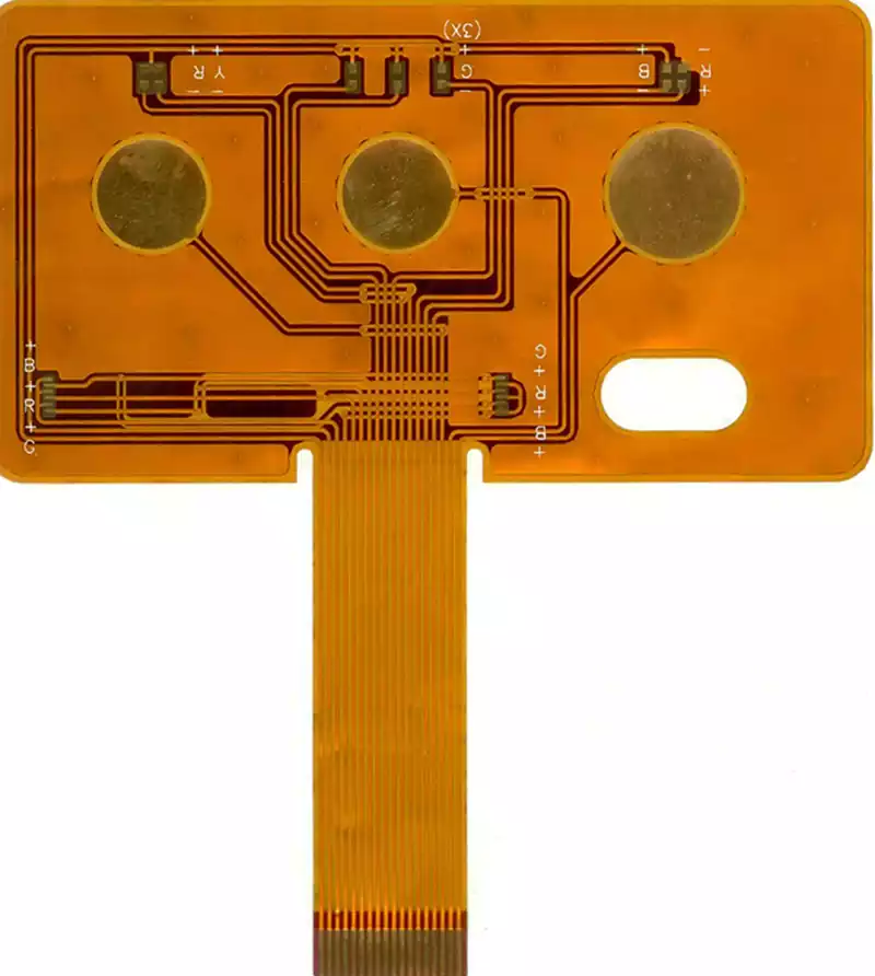
Characteristics: Thickness controllable within 0.1mm, offering optimal flexibility. However, the single-layer structure imposes constraints on layout space, making it suitable only for simple, low-density circuits (e.g., keypads, LED connections).
Double-Layer flexible printed circuit boards
Construction: Comprises five laminated layers: coverlay, top copper foil, substrate, bottom copper foil, and coverlay. Electrical interconnection between layers is achieved via plated-through holes (vias) formed through laser or mechanical drilling.
Characteristics: Thickness increases to 0.2–0.3mm, with slightly reduced flexibility. However, routing density improves by over 50%, enabling support for moderately complex circuits (e.g., camera modules, sensor connections).
High-layer flexible printed circuit boards
Construction: Employing three or more conductive layers, achieved by alternately laminating inner core layers with outer copper foils. Utilises blind via and buried via technologies for multi-layer interconnection.
Characteristics: Thickness may exceed 0.5mm, limiting flexibility. However, routing density increases 3-5 times, supporting high-speed signal transmission (e.g., 5G antennas, server backplanes). This constitutes the core connectivity solution for high-end electronic devices.
- Layout and Routing Differences
① Routing Space and Layer Count
Single-layer flexible printed circuit boards: Single-sided routing requires jumper wires or 0-ohm resistors for line crossovers, resulting in low routing efficiency. Suitable only for simple designs with <50 lines.
Double-layer FPC: Double-sided routing utilises vias for interlayer connections, doubling routing density. Supports 100-300 lines, meeting medium-complexity requirements.
Multi-layer FPC: Multi-layer routing enables separation of signal, power, and ground planes. Achieves routing densities exceeding 500 traces/cm², facilitating high-speed differential pairs (e.g., USB 3.0, HDMI) and interconnections with high-density BGA packages.
② Via Implementation
Single-layer FPC: No via design; trace connections rely solely on single-sided routing, requiring clearance space at intersections.
Double-layer FPC: Utilises mechanical drilling + electroplating to form vias with ≥0.15mm diameter, requiring controlled wall roughness to minimise signal loss.
Multi-layer FPC: Incorporates laser blind vias (≤0.1mm diameter) and backdrill processes to eliminate stubs, reducing signal distortion below -40dB.
③ Signal Interference Mitigation
Single-layer FPC: Concentrate signal traces. Isolate sensitive lines via ground planes or hatch ground patterns to reduce coupling interference.
Double-layer FPC: Isolate signals using inner power/ground planes. Optimise high-speed signal transmission (e.g., MIPI, LVDS) through coplanar waveguide (CPW) structures.
Multi-layer FPC: Employ symmetrical stack-up structures (e.g., Signal-GND-PWR-Signal) to control characteristic impedance at 50±10%. Route critical signals on inner layers and utilise electromagnetic shielding film to reduce radiation.
④ Manufacturing Process Requirements
Single-layer FPC: Simple process, low cost, suitable for mass production.
Double-layer FPC: Requires additional processes such as via fabrication and electroplating, resulting in higher costs but enabling greater circuit integration.
Multi-layer FPC: Involves complex manufacturing processes including multi-layer printing and assembly techniques, presenting significant production challenges and high costs. However, advanced technologies like roll-to-roll (R2R) processes can enhance mass production efficiency and reduce costs.
The distinction between single-layer and double-layer flexible printed circuit boards structures in layout and routing fundamentally represents a trade-off between space utilisation and design complexity. Single-layer flexible pcb firmly dominate markets for straightforward applications through their minimalist construction and cost advantages. Conversely, double-layer flex pcb demonstrate greater integration flexibility in moderately complex circuits by incorporating via design and dual-sided routing capabilities.