Chip packaging technology constitutes a critical component within the semiconductor industry, directly influencing the performance, reliability, and lifespan of electronic devices. In recent years, as electronic products have evolved towards miniaturisation and enhanced performance, traditional packaging materials have progressively revealed their limitations. Against this backdrop, glass substrates, owing to their unique physicochemical advantages, are increasingly emerging as the preferred choice within the chip packaging sector.
Composition Systems and Physical-Chemical Properties of Glass Substrates for Chip Packaging
Composition Systems for Glass Substrates The composition systems for glass substrates used in chip packaging primarily encompass borosilicate glass systems, aluminosilicate glass systems, and alkali-free alumino-borosilicate glass systems. Borosilicate glass substrates typically contain approximately 80% by mass SiO₂ and 12%–13% B₂O₃. This glass system offers advantages such as excellent thermal resistance, a low coefficient of thermal expansion, and high chemical stability. The thermal expansion coefficient of borosilicate glass substrates matches that of silicon chips, providing excellent thermal stability. This prevents warping deformation caused by chip heat generation or circuit connection failure, making it highly suitable for electronic packaging demanding superior thermal stability.
Aluminosilicate glass substrates primarily comprise SiO₂ and Al₂O₃, alongside alkali metal oxides (R₂O) and alkaline earth metal oxides (RO). This glass system exhibits outstanding optical properties, hardness, low surface tension, and a low thermal expansion coefficient. Aluminosilicate substrates are suitable for electronic packaging applications requiring high mechanical strength and wear resistance.
Alkali-free aluminosilicate glass substrates contain extremely low levels of alkali metal oxides, typically not exceeding 0.1% by mass. This substrate exhibits outstanding electrical insulation properties, effectively preventing electrical signal interference and leakage, making it highly suitable for encapsulating high-frequency electronic components. Furthermore, alkali-free aluminosilicate glass substrates demonstrate excellent corrosion resistance in acids, alkalis, and organic solvents, maintaining stable physical and chemical properties over extended periods. Owing to their absence or minimal presence of alkali metal oxides, these glass substrates possess favourable chemical stability and electrical insulation properties, enabling resistance to external impacts and mechanical stresses. Alkali-free aluminosilicate glass substrates are frequently employed in microelectromechanical system (MEMS) devices such as accelerometers, gyroscopes, and pressure sensors, which demand stringent requirements for high mechanical strength and low thermal expansion coefficients.
Glass substrates for chip packaging must exhibit outstanding physical and chemical properties, including dielectric characteristics, thermal expansion coefficient, mechanical strength, optical properties, and etchability. These attributes not only influence substrate processing and application but also directly impact the overall performance of packaged electronic devices. The following sections will explore the critical physical and chemical properties required for glass substrates in practical applications and their effects on electronic device performance.
Dielectric constant The dielectric constant serves as an indicator of a glass material’s capacity to store electrical charge within an electric field. A higher dielectric constant may result in signal delay or distortion. In high-frequency signal transmission, glass substrates with a low dielectric constant offer advantages over silicon substrates. Furthermore, an excessively high dielectric constant increases parasitic capacitance, thereby impacting circuit performance (such as signal integrity and signal transmission speed). Consequently, glass substrates with low dielectric constants are more suitable for high-frequency electronic components, such as applications in microwave and radio frequency fields.
Dielectric loss measures a glass material’s capacity to dissipate electrical energy within an electric field. The tangent of the loss angle (tan δ) serves as a quantitative indicator of dielectric loss, representing the ratio of energy dissipation to energy storage at a specific frequency. Low dielectric loss implies reduced energy dissipation under electric fields, thereby enhancing device energy efficiency. Conversely, high dielectric loss causes signal attenuation during transmission, compromising signal strength and quality while generating increased heat, necessitating superior thermal management. Professor Zhang Jihua’s team at the University of Electronic Science and Technology of China significantly reduced the dielectric loss of photosensitive glass by leveraging the neutralisation effect, suppression effect, and stabilisation effect. The developed photosensitive glass exhibits a dielectric loss tangent of merely 1‰ to 2‰ at 500 MHz, with a photosensitive wavelength range of 310 to 320 nm. Compared to the sole commercially available photosensitive glass, Schott Foturan II, this novel material demonstrates over 50% lower dielectric loss, rendering it particularly suitable for semiconductor packaging applications.
Thermal Expansion Coefficient The thermal expansion coefficient of glass substrates must match other packaging materials to minimise deformation caused by thermal effects. A low thermal expansion coefficient ensures the glass substrate maintains stable shape and dimensions during prolonged use, reducing stress accumulation and enhancing the reliability of electronic devices.
Mechanical Properties The mechanical properties of glass substrates determine the reliability of the encapsulation structure. Lower-density glass substrates effectively reduce device mass while maintaining sufficient mechanical strength. Modulus of elasticity measures a material’s resistance to deformation; a higher modulus ensures substrate stability during encapsulation, reducing failure risks. Vickers hardness reflects a material’s scratch resistance and wear resistance. High-hardness glass substrates enhance the durability of the encapsulation. Fracture toughness indicates a material’s resistance to fracture during crack propagation. Higher fracture toughness prevents cracking in the substrate under stress, ensuring the integrity and stability of the encapsulation.
Optical Properties
During the encapsulation of optical and electronic devices, glass substrates may undergo mechanical stresses that alter their optical characteristics, thereby affecting light signal transmission and device performance. Concurrently, glass substrates must exhibit high light transmittance to ensure efficient optical signal propagation.
Etching Performance
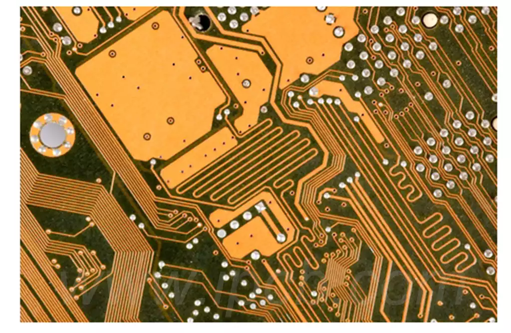
Through-glass via (TGV) processing typically employs laser-induced etching technology for hole formation. The TGV process creates fine through-hole structures on the glass substrate, providing pathways for electrical interconnections within chip packaging. This process involves laser drilling holes in the glass substrate, followed by deposition of a Ti/Cu seed layer, electro/chemical plating of Cu, and finally surface planarisation via chemical mechanical polishing. The etch rate of hydrofluoric acid is critical in TGV processing. An appropriate etch rate ensures the formation of through-holes with high aspect ratio and verticality. Smooth hole walls reduce resistance and capacitive effects, enhancing signal transmission stability and speed. Proper control of the etch rate also improves processing efficiency, minimises polishing and cleaning steps, and optimises the overall process flow.
The Critical Role of Glass Substrates in Chip Packaging
- Structural Support Provided by Glass Substrates
The primary function of glass substrates in chip packaging is to provide structural support. Owing to the exceptional hardness and flatness of glass material, it offers a robust foundation for fragile chips. This support ensures the stability of the chip during packaging and usage, preventing damage caused by physical impact. - Protecting Chips from Environmental Damage
Beyond structural support, glass substrates effectively shield chips from external environmental hazards. Their smooth surface and superior barrier properties prevent moisture, dust, and other contaminants from reaching the chip, thereby preserving its performance and lifespan. This protective function is particularly crucial in humid or dusty environments. - Functioning as a heat sink for thermal dissipation
High-performance chips generate significant heat during operation. Without timely dissipation, this heat can impair chip performance or cause damage. Glass substrates, owing to their excellent thermal conductivity, serve as heat sinks, facilitating more efficient heat removal and ensuring stable chip operation.
Trends in Glass Substrate Development
Thinner and lighter designs: As electronic products increasingly pursue slimness and lightness, demands on packaging materials grow ever more stringent. Future glass substrates will evolve towards greater thinness and lightness to meet these demands.
High Performance: To enhance semiconductor device capabilities, glass substrates require continuous optimisation of their optical, thermal, and electrical properties. This includes developing novel materials with high light transmittance, low thermal expansion coefficients, and superior electrical insulation.
Environmental Sustainability: With heightened environmental awareness, future glass substrate production will prioritise eco-friendliness and sustainability. This includes adopting environmentally conscious materials and manufacturing processes to reduce energy consumption and waste emissions during production.
Intelligent and Multifunctional Capabilities: Driven by rapid advancements in technologies such as the Internet of Things and artificial intelligence, future glass substrates may integrate additional functionalities like touchscreens and displays, enabling smarter semiconductor packaging solutions.
Challenges Facing Glass Substrates
Despite numerous advantages in semiconductor packaging, glass substrates confront several challenges.
Cost Concerns: Compared to organic materials, glass substrate production incurs relatively higher costs. This may limit their application in certain low-cost products. To mitigate expenses, approaches such as refining production processes, enhancing efficiency, and utilising recycled materials could be explored.
Processing Difficulty: Whilst glass substrates exhibit favourable machinability, certain specialised processes—such as precision drilling and ultra-thin cutting—present technical challenges. Addressing these requires developing novel processing technologies and equipment to enhance machining accuracy and efficiency.
Fragility Concerns: Whilst exhibiting high hardness, glass substrates correspondingly display a degree of brittleness. This may lead to breakage during processing, transportation, and installation. To address this, novel toughening techniques such as composite materials and surface treatments can be explored to enhance the impact resistance of glass substrates.
Glass substrates demonstrate significant application potential in semiconductor packaging due to their outstanding properties. Despite challenges such as cost, driven by trends towards thinning, high performance, environmental sustainability, and intelligent multifunctionality, glass substrates are poised to play an increasingly vital role in future chip packaging.