The Foundation of the Integration of Drones PCB Systems
As highly integrated intelligent flight platforms, drone pcb have evolved from their original military reconnaissance tools to comprehensive systems widely used in a variety of fields, including aerial photography, logistics, agricultural monitoring, surveying and mapping, and even emergency rescue. Their complex flight control, navigation, image processing, and communication functions all rely on high-performance electronic systems. The “heart” of these electronic systems is the printed circuit board (PCB), responsible for signal transmission and power distribution.
Stable drone flight requires real-time processing of massive amounts of sensor data, including accelerometers, gyroscopes, barometers, GPS modules, and image sensors. This data is transmitted within milliseconds via the PCB to the main control chip, where it is then processed by the flight control algorithm and output to the motor drive module. Every signal delay, noise interference, or wiring mismatch can affect the drone’s flight attitude and control accuracy. Therefore, PCB design is not just a matter of electronic layout but also a key technology for flight safety and performance.
As drones continue to become smaller and more intelligent, their internal circuit density continues to increase. In the past, single- or double-layer PCBs were no longer sufficient for the wiring requirements of complex systems. Today, main control and power modules generally adopt multi-layer structures with four to ten layers to achieve high-speed signal transmission and precise power distribution. Furthermore, to accommodate complex structural layouts, flexible printed circuits (FPCs) are widely used in aircraft arms, camera gimbals, and sensor connections, reducing overall weight and increasing space efficiency.
Furthermore, drones operate in extremely complex environments, potentially flying at high altitudes and in low temperatures, as well as in high humidity and high heat. This places even stricter demands on PCB reliability. Materials must possess excellent heat resistance, oxidation resistance, and mechanical strength, while maintaining signal integrity under high-frequency operating conditions. Improper design or process control can lead to microcracks caused by thermal expansion and contraction, copper foil delamination, or solder joint fatigue, all leading to system failure.
The PCB is not only the supporting structure for drone circuits but also an invisible determinant of flight performance and safety. The wiring design, material selection, and manufacturing precision of each board are fundamental to a drone’s stable operation in complex environments.
Common types of drone PCBs
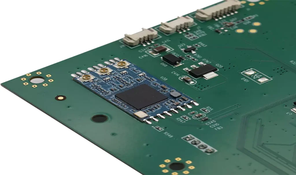
Flight control core board: Houses the main processor, sensors, memory and other components that form the core of the flight control system. It has the highest requirements for signal integrity and reliability. 2. Power distribution board: Efficiently and stably distributes battery power to various modules such as ESCs, flight controllers and video transmission systems. It needs to handle high currents, requiring thick copper foil and high-current routing.
ESC Board: A circuit board that controls motor speed, comprising an MCU, MOSFET driver bridges, current sensing circuits, etc. It must handle high-power, high-frequency switching currents and thermal management.
Video Transmission Transmitter Board: A circuit board that processes and transmits video signals, comprising a video processor, wireless RF modules, etc. It involves high-speed video signal and RF design.
Receiver Board: A module for receiving remote control signals.
GPS/RTK Module Board: A module board containing a GPS/GNSS receiver chip and an antenna.
Vision/Obstacle Avoidance Module Board: A board containing cameras, ultrasonic sensors, TOF sensors and their associated processing circuits.
The Role and Function of the PCB—the Core of a Drone’s Main Control System
In a drone’s electronic system, the main control unit (MCU) is considered the “brain,” while the PCB serves as the “central channel” that runs through the entire neural network. It not only hosts all core chips, sensor modules, and interface components, but also handles high-speed signal transmission, power distribution, and system grounding. Whether it’s a miniature recreational drone or an industrial platform equipped with multiple sensors, the PCB plays an indispensable role.
The core of the MCU typically includes the flight controller unit (FCU), image processing module, communication module, and power management unit. These components are highly integrated on the motherboard, with complex signal routing and electrical isolation enabling multi-module coordination. The flight controller receives real-time data from sensors such as the gyroscope, accelerometer, magnetometer, and GPS. After algorithmic calculations, it outputs control signals to the electronic speed controller (ESC), which then drives the motor to adjust speed to maintain flight stability. In this process, the PCB serves as both a data transmission medium and a current distribution channel. Any trace impedance mismatch or power supply ripple interference can cause flight control anomalies.
Unlike traditional consumer electronics, the biggest challenges facing drone PCBs are real-time performance and interference immunity. During flight, there’s often less than 10 milliseconds of latency between signal transmission from sensors to control chips and their execution. To avoid latency accumulation and jitter, designers must optimize timing during the PCB layout phase, minimizing the path length of critical control lines and reducing crosstalk and noise interference through differential signaling, impedance matching, and ground isolation. This is especially true in high-speed data channels, such as the MIPI or LVDS signal interfaces used by image transmission modules. Any slight imbalance can cause image distortion or increased latency.
Power distribution is also a key concern in drone PCB design. The flight control, motor drive, image processing, and wireless communication modules all have distinct voltage and current requirements. The copper width, trace routing, and number of vias on the PCB directly impact power supply stability. Therefore, high-performance drones typically integrate a multi-stage power management system on the motherboard and utilize multi-layer power and ground plane structures to minimize electromagnetic interference and maintain uniform power transmission. Furthermore, thickened copper foil or localized metal reinforcement layers are often used for high-current paths to prevent voltage drops or localized heating during high-power motor startup.
The communications module is another module that places high demands on the PCB. Drones rely on wireless links for remote control and image transmission, typically operating in the 2.4GHz to 5.8GHz frequency range. To ensure signal quality, the PCB layout of the radio frequency (RF) section must strictly control impedance and path length. Ground shields must be provided between sensitive and digital areas to prevent digital noise from intruding into the RF module. High-end drones even use independent RF daughterboards, connected to the main board via RF connectors, to further enhance signal purity and transmission stability.
Furthermore, the main control PCB is responsible for system monitoring and self-protection. It incorporates temperature sensors, current sensing resistors, and voltage monitoring circuits to monitor the entire device’s operating status in real time and trigger automatic protection or emergency landing procedures in the event of anomalies. To achieve these functions, the design often requires integrating a large number of surface-mounted device (SMD) components within a limited space while ensuring unobstructed heat dissipation. The high-density layout requires extremely high manufacturing precision, while also challenging soldering quality and assembly tolerances. In general, the design of a main control system PCB involves more than just implementing electrical connections; it’s a comprehensive engineering process involving the coupling of multiple physical fields. From signal integrity and electromagnetic compatibility to thermal management and mechanical structure, every detail impacts the performance and reliability of a drone. For this reason, the main control PCB is considered the most technically demanding component of a drone system, and its design quality often directly reflects the manufacturer’s engineering capabilities and product competitiveness.
Drone PCB Design Considerations and Challenges
The core of a drone lies not only in its propulsion system and flight control algorithms, but also in the PCB design—the “neural network” that supports the entire system. An excellent drone PCB must implement multiple functions, including signal processing, power distribution, data transmission, and communication, within a limited space, placing extremely high demands on designers.
Balancing Lightweight and High Density
Drone endurance is often directly affected by weight, so lightweighting is a primary goal in PCB design. Designers typically use high-TG fiberglass materials (such as FR-4 TG170 or higher) or polyimide (PI) flexible boards to reduce weight while maintaining sufficient strength and thermal stability.
However, lightweighting does not necessarily mean sacrificing electrical performance. Drone circuit systems, including control boards, electronic control boards, GPS modules, and image transmission boards, feature numerous complex functions and dense signals. Arranging so many components within a limited area requires increased circuit density and layer count.
This is why multi-layer boards (6, 8, or even 12 layers) are becoming increasingly common in mid- to high-end drones. A well-defined layer stackup (such as a symmetrical signal-ground-power-signal layout) can reduce electromagnetic interference (EMI) and optimize signal integrity while maintaining mechanical strength.
Power Distribution and Thermal Management
Drone power consumption is highly unevenly distributed. Power systems (such as motors and electronic control boards) draw instantaneous currents of tens of amperes, while control systems and image transmission modules require extremely high voltage stability.
Thus, power layer design and copper thickness control are critical. High-current areas typically use 2 oz or greater copper thickness to minimize voltage drop and heat generation, while signal layers require thinner copper thicknesses to ensure impedance stability.
Thermal management is another major challenge in drone PCB design. During flight, drones operate within confined spaces, with limited airflow and poor heat dissipation. Common optimization methods include:
Designing thermal vias beneath high-power components; using copper foil to dissipate heat in the power supply area; and, when necessary, using metal-on-carbon printed circuit boards (MCPCBs) or ceramic substrates for LED lighting or power conversion modules.
Furthermore, thermal simulation analysis is particularly important during the design phase. Predicting temperature rise using software (such as ANSYS or Altium Designer’s thermal simulation capabilities) can effectively prevent solder joint fatigue or chip damage caused by localized overheating.
Electromagnetic Compatibility (EMC) and Signal Integrity
Drones typically integrate multiple high-frequency communication modules: GPS, Wi-Fi, Bluetooth, 5.8GHz image transmission, and even 4G/5G modules. Improper handling of these RF signals can easily lead to crosstalk and radiation interference, compromising flight control and communication stability.
Key design considerations include:
Separate RF and digital signal routing to avoid mutual interference; implement impedance control and equal length design for high-speed signal lines (such as SPI, MIPI, and HDMI); add ground rings and shielding layers around RF modules to reduce external interference; and use filter capacitors and ferrite beads to isolate power supply noise in the electronic speed controller (ESC) and motor drive components.
To prevent electromagnetic interference caused by transient current fluctuations during takeoff, acceleration, or attitude adjustments, engineers typically implement decoupling capacitor arrays and analyze ground plane integrity to maintain stable system operation.
Vibration Resistance and Reliability Design
Drones are frequently subjected to vibration and impact during flight. Improper PCB design can easily lead to problems such as loose solder joints, cracked traces, and layer separation. Common protection strategies include:
Using reinforced vias or widened ring pads in critical connection areas (such as the flight control and motor interfaces);
Using Rigid-Flex structures for flexible connections, which provides both vibration resistance and ease of layout;
Coating the entire PCB with conformal coating (moisture-proof, salt spray-proof, and corrosion-resistant);
Using underfill to enhance the vibration resistance of BGAs and chip modules.
In addition, high-reliability drones (such as those used for surveying, inspection, and military applications) typically require PCBs to meet IPC-6012 Class 3 standards to ensure mechanical strength and electrical stability under long-term use.
Signal Latency and Data Synchronization
As drone functionality expands, high-precision synchronization is required between modules such as image transmission, positioning, flight control, and obstacle avoidance. PCB trace design must consider signal skew and timing alignment.
For example, inconsistent MIPI signal latency from the camera to the host controller can cause image freezes or frame drops. Designers use differential signal routing and time-domain simulation tools for optimization. In addition, the high-speed communication between the FPGA and MCU also places strict demands on trace timing matching. These details often determine whether a drone can fly stably in complex environments.
Drone PCB Manufacturing and Assembly Process
Design is only the first step in the lifecycle of a drone PCB. Manufacturing and assembly are the key links that truly determine its performance and reliability. During the production process, drone PCBs must simultaneously meet the requirements of high-precision routing, high-layer stacking, strict impedance control, and reliable assembly, which poses significant challenges to the factory’s manufacturing capabilities and process stability.
Manufacturing Process Overview
The manufacturing process for drone PCBs is similar to that of ordinary multilayer boards, but requires higher levels of process control precision. The main steps include:
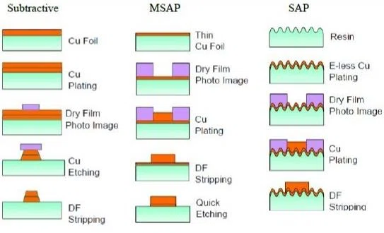
Inner Layer Etching: According to the design documents, the inner layer copper foil is exposed, developed, and etched to form the circuit. The line width and spacing control at this stage directly affects signal integrity.
Lamination: The multiple layers of circuit boards are stacked together, and the resin is flowed and cured under high temperature and high pressure to form a unified multilayer structure. Drone PCBs often include power and ground layers, and the lamination pressure and temperature profile requirements are extremely strict.
Drilling & Plating: Drilling accuracy determines the stability of the signal path. Laser via technology is often used in blind/buried via structures to improve space utilization. Subsequent electroless copper plating and electroplating ensure reliable interlayer conductivity.
Outer Layer Patterning: Dry film lithography and etching processes are used to create the outer layer traces, while ensuring that copper thickness variations caused by uneven etching are avoided.
Solder Mask & Silkscreen: Drone PCBs often use matte green solder mask ink to improve optical recognition accuracy. For high-frequency signal areas, uniform solder mask thickness is required to avoid impedance variations.
Surface Finish: Common processes include ENIG (electroless nickel tinned gold), OSP (organic oxide semiconductor plating), and immersion silver. ENIG is often used for drone main control boards to improve soldering reliability and oxidation resistance.
Electrical Testing and Appearance Inspection (E-Test & AOI): Flight control PCBs require 100% electrical continuity testing, combined with automated optical inspection (AOI) and X-ray inspection to prevent hidden defects such as shorts, opens, and broken copper within vias.
Every step is crucial, as even the slightest error can lead to catastrophic consequences during flight.
Key Process Controls
Layer Alignment Accuracy. Drone PCBs typically have 6 to 12 layers, and the tolerance for multi-layer alignment deviation is extremely low. Layer misalignment exceeding ±75μm can cause signal path distortion or uneven power distribution.
Modern factories use CCD automated alignment systems and vacuum lamination equipment to ensure stacking accuracy and air bubble removal, preventing delamination and voids.
Microvia Plating Reliability. Due to the limited space in drones, HDI structures are widely used. Laser microvias (typically 0.1mm–0.15mm in diameter) are most prone to “hollow holes” or “thin edges” during the plating process. To avoid this problem, vertical electroless copper plating equipment (VCP line) and additive-based precision plating processes are required to ensure hole wall uniformity and conductivity.
Impedance Control and Testing. Drone image transmission, radar, and navigation modules involve high-frequency signal transmission, so impedance errors must be controlled within ±5%.
Prior to production, factories must produce impedance test coupons to verify the consistency of dielectric thickness, copper thickness, trace width, and dielectric constant.
If there are material batch differences or press fit deviations within a production batch, the impedance model must be recalibrated; otherwise, RF performance will be directly affected.
Cleanliness and Anti-static Control. Drone PCBs are often used in outdoor environments, requiring extremely high cleanliness standards. Residual flux ions or dust particles can cause surface leakage or corrosion.
Manufacturers typically use a combination of plasma cleaning and ultrasonic cleaning to ensure surface cleanliness that meets IPC-TM—650 standards.
In addition, all assembly workshops must maintain an electrostatic protection level below Class 10000 to prevent damage to sensitive components from electrostatic discharge (ESD).
Assembly and Soldering Technology
The assembly process of drones directly determines the reliability of the entire device. Compared to traditional electronic products, assembly is more challenging for several reasons:
The components are small and dense; there is a high concentration of mixed flexible and rigid boards; and after soldering, they must withstand vibration and temperature cycling.
SMT placement. Drone motherboards typically use micro-packaged components such as 0201 and 01005, requiring extremely high placement accuracy. High-end factories use vision positioning systems (AOA) and laser alignment cameras to ensure component positioning deviations do not exceed ±25μm.
Solder paste printing thickness must be strictly controlled between 0.10–0.12mm to avoid bridging or cold solder joints.
Reflow control. Drone PCBs contain copper layers of varying thicknesses and a mixed base material, resulting in uneven temperature distribution. To avoid thermal shock, a multi-zone temperature-controlled reflow oven is typically used, and a profiler monitors the temperature rise of each layer in real time.
Common defects such as “head-in-pillow” and “cold solder joints” must be addressed during the manufacturing process through profile optimization and nitrogen protection.
Post-soldering and assembly: Load-bearing components such as power connectors and motor interfaces are typically reinforced using wave soldering or manual soldering. Epoxy reinforcement is applied to critical solder joints to enhance vibration resistance.
After assembly, functional testing (FCT) is also required, including voltage distribution, signal response, wireless communication stability, and image transmission delay testing.
Quality Inspection and Reliability Verification
Drone PCBs must undergo a rigorous quality control process to ensure long-term stable operation:
X-ray inspection: used to check for voids and solder joint quality on BGA and CSP solder joints; ICT (In-Circuit Test) testing: checks component assembly accuracy and open and short circuit conditions; Thermal Cycling testing: verifies the PCB’s thermal fatigue resistance under repeated temperature fluctuations from -40°C to +85°C; Vibration and Drop Testing: simulates flight vibrations and drop shock; Salt Spray and Humidity Aging Testing: verifies the long-term protective effects of the three-component coating.
Only PCBs that pass this comprehensive test can be used in drone main control or electronic speed control systems.
Typical Manufacturing Problems and Optimization Directions
Common issues in drone PCB production include:
Lamination bubbles and delamination → Improve vacuum lamination and resin flow control; Solder mask shift → Improve exposure accuracy and use an automated calibration system; Uneven or broken copper in vias → Optimize plating recipes and mixing methods; Warpage → Control through symmetrical stacking and low-stress substrates; Impedance deviation → Strictly monitor dielectric thickness and material batches.
In the future, drone PCB manufacturing is moving towards automation, intelligent inspection, and traceability. Through MES systems, AI-powered visual inspection, and big data process analysis, manufacturers can predict failure trends in advance, achieving higher yields and consistency.
Development Trends and Future Technology Directions for Drone PCBs
The drone industry is entering a new era centered on intelligence, lightweighting, and high reliability. As the carrier of drone electronic systems, PCB design and manufacturing technologies are constantly evolving to address multiple challenges such as performance upgrades, size reduction, heat dissipation complexity, and cost optimization. From materials to structures, from manufacturing to inspection, drone PCBs are evolving towards higher density, higher frequency, and higher reliability.
Trends in Lightweighting and High Integration
A drone’s flight endurance is closely tied to its weight, and the PCB is a crucial component of the entire device. Traditional FR-4 materials have reached bottlenecks in terms of mechanical strength, dielectric properties, and weight, making material innovation a key breakthrough.
Currently, the industry is gradually shifting toward lightweight, high-strength substrates, such as low-density composites with lower glass fiber content, ceramic-filled resin substrates, and even hybrid structures with metal-based and composite layers. These materials reduce weight while maintaining high thermal conductivity, thereby improving overall heat dissipation performance. Furthermore, multilayer boards are evolving into system-in-package (SiP) and embedded component PCBs, where some chips, resistors, and capacitors are embedded directly within the board, achieving circuit miniaturization and structural integration.
This trend toward high integration not only reduces assembly costs but also improves signal transmission efficiency and reduces interconnection losses, resulting in faster drone control response and lower system latency. For commercial drones, this improvement means longer flight range and more precise control while maintaining the same power consumption.
Increasing Application of High-Frequency, High-Speed Design
With the advancement of drone communication and perception systems, high-frequency, high-speed signal design is becoming a major focus in PCB development. High-definition image transmission, 5G remote control links, millimeter-wave radar, laser ranging, and AI vision systems all require stable operation at higher bandwidths.
To meet these demands, drone PCBs are gradually incorporating high-speed material systems, such as Rogers, Panasonic Megtron, Taconic, and Isola high-frequency copper-clad laminates. These materials offer low dielectric constants (Dk) and low dielectric loss (Df), effectively reducing signal attenuation and latency.
In addition, designers are optimizing signal integrity through differential pair routing, controlled impedance, and multi-point grounding techniques. For high-end drones, PCB trace accuracy has reached sub-100μm levels, requiring manufacturers to maintain extremely high levels of process control.
In the future, with the introduction of AI vision algorithms and edge computing, data processing modules will require interconnect architectures with higher bandwidth and lower latency. PCB design will further integrate with packaging technology, developing new forms such as multi-layer 3D PCBs and arbitrary layer interconnect (HDI) structures, providing drones with enhanced computing and communication capabilities.
Thermal Management and Power Optimization
The compact structure and complex functionality of drones lead to concentrated heat generation in the system. This is especially true for high-power components such as the flight control motherboard, motor drivers, power management chips, and image processors, which generate significant heat in a short period of time. Improper heat dissipation can severely impact circuit stability and component lifespan.
Traditional heat dissipation methods rely on metal heat sinks or thickened copper foil, but this increases weight and compromises design flexibility. Newer generation drone PCBs are incorporating metal-based heat dissipation layers (MCPCBs), thermally conductive filler resins, and thermal via arrays (TVAs). These structures significantly improve thermal conductivity while maintaining lightweight, allowing heat to be quickly distributed throughout the board or structural frame.
Additionally, the introduction of a distributed power balancing network (PDN) in the power plane ensures uniform power supply and reduces voltage fluctuations, further minimizing losses caused by localized heat generation.
In the future, hybrid heat dissipation technology, incorporating carbon-based materials (such as graphene thin layers) or ceramic substrates, will become a new direction for drone PCB thermal management. This technology not only addresses the thermal bottlenecks associated with high-density integration but also provides a viable path for high-power applications such as industrial mapping and long-endurance drones. Widespread Adoption of Flexible and Rigid-Flex Structures
To meet the increasingly complex structural layouts and lightweight requirements of drones, flexible printed circuits (FPCs) and rigid-flex PCBs are widely used in flight control systems, gimbals, sensor connections, and image modules.
Flexible circuits allow for three-dimensional wiring within limited spaces, greatly increasing internal layout flexibility. For example, a foldable flexible cable can connect the camera module to the main control unit, saving space and reducing the number of signal plug-in interfaces. Rigid-flex technology achieves an optimal balance between structure and function by retaining rigid areas (for component mounting) in key locations and using flexible sections (for signal transmission and folding) elsewhere.
As drones become more modular and miniaturized, flexible circuits not only reduce weight but also effectively resist flight vibration, improving system reliability. In the future, this trend will be combined with 3D printing and flexible packaging technologies to create lighter and more durable drone electronic architectures.
Smart Manufacturing and Quality Traceability
At the manufacturing level, traditional manual inspection and segmented management are no longer sufficient to meet the production demands of high-density drone PCBs. The industry is gradually moving towards smart manufacturing and closed-loop data management.
Through the MES (Manufacturing Execution System), the entire process of each PCB, from material warehousing, pressing, drilling, plating, mounting, to final testing, is digitally recorded, enabling full lifecycle traceability. AI-powered visual inspection systems can identify solder joint defects and broken traces in milliseconds, while SPC statistical process control technology enables real-time adjustment of key process parameters to ensure batch consistency.
Furthermore, drone PCB manufacturers will leverage digital twin technology to achieve virtual simulation production, predicting yield and failure modes during the design phase, thereby reducing actual trial production costs. The integration of blockchain technology to store quality data on-chain is also expected to be widely adopted in high-end aerial photography and military drones.
Green and Sustainable Manufacturing
With increasing global attention to carbon emissions and sustainable development, the PCB industry is actively responding. Drone manufacturers are seeking solutions using halogen-free materials, low-VOC inks, and recyclable substrates to reduce environmental impact.
Advanced factories use closed-loop water treatment systems and copper recovery electrolysis processes to recycle metal ions from wastewater and residual liquids, reducing pollution. Furthermore, the use of lead-free soldering and energy-saving reflow equipment is also reducing energy consumption and carbon footprint. In the future, environmental standards will become one of the market entry barriers for drone PCB manufacturing, making green production no longer an option but an inevitable trend.
Future Outlook
Drone technology is evolving at a rate far faster than that of the traditional electronics industry, and PCBs are the foundational platform supporting this transformation. From high-frequency communications to AI control, from flexible structures to intelligent manufacturing, each iteration of drone PCBs represents a leap forward in the field of electronic engineering.
As the global market continues to expand drone applications—from aerial photography and surveying and mapping to logistics, agriculture, security, and energy inspection—the performance requirements for circuit boards will continue to rise. Future drone PCBs will not only be a means of electronic connectivity but also the functional core of intelligent systems. In the near future, we may see “smart PCBs” with self-diagnosis, adaptive adjustment, and energy recovery capabilities. These will make drones more efficient and reliable, bringing them closer to the ultimate form of “flying computing platforms.”
Conclusion
A drone’s flight performance, data processing capabilities, and control precision ultimately depend on the circuit boards hidden beneath its fuselage. Drone PCBs are not only a platform for electronic components but also the core foundation for the entire device’s intelligence, reliability, and lightweight design. They perform multiple functions, including signal transmission, power distribution, thermal management, and structural support, serving as a bridge connecting “flight” and “intelligence.”
From a design perspective, the development of drone PCBs has already broken through the boundaries of traditional circuit boards. The application of high-density interconnect (HDI), rigid-flex structures, and embedded component technologies has transformed circuits from two-dimensional surfaces into three-dimensional system carriers. From a manufacturing perspective, the widespread adoption of microvia plating, vacuum lamination, automated optical inspection, and intelligent assembly has continuously improved the reliability of drone PCBs. Every process optimization strengthens flight safety.
However, the evolution of drone PCBs is far from over. With the convergence of AI algorithms, big data processing, edge computing, and 5G communications, future circuit boards will no longer be just “hardware” but intelligent modules with data awareness. They will possess self-detection capabilities, adjustable impedance structures, and adaptive energy control systems, achieving true “smart circuits.”
In the future, whether it’s aerial photography drones, mapping drones, or high-precision industrial drones, PCB technology will become a core competitive advantage. Only companies that can continuously break through in materials, processes, and system integration will have the opportunity to seize a leading position in this rapidly growing market.
The story of the Drone PCB is a microcosm of the integration of modern manufacturing and intelligent technology. It demonstrates that every tiny technological advancement can potentially translate into a more stable and intelligent flight at thousands of meters in the air.