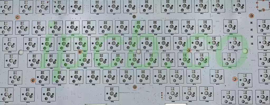
In single-sided board designs, only one side features copper foil traces (i.e., the solder side), with electronic components placed exclusively on the opposite side (i.e., the component side). In double-sided and multilayer boards, both sides contain copper foil traces and can accommodate surface-mount devices (SMDs). Here, the ‘component side’ typically denotes the side housing the primary, complex, or greater number of components (usually the Top Side), while the ‘solder side’ refers to the opposite side (usually the Bottom Side).
SMD double-sided placement: In modern high-density designs, SMD electronic components are placed and soldered on both sides. In such cases, the term ‘solder side’ becomes less precise. More universal terminology is Top Layer and Bottom Layer:
Top Layer: Typically serves as the default primary component side.
Bottom Layer: Also carries components, with soldering performed on this side (reflow soldering).
Differentiation based on electronic component layout and type
Characteristics of the Primary Side (Component Side)
Concentration of core electronic components: Critical elements such as CPUs, chipsets, large ICs, connectors (e.g., USB, HDMI interfaces), and slots (e.g., memory slots, PCIe slots) are generally positioned on the primary side.
High Component Density: The primary side accommodates numerous functional modules, featuring denser electronic component arrangements. Multi-layer stacked components may occur, such as small capacitors positioned beneath BGA chips.
Visible Markings: Electronic component surfaces may bear printed brand names, model numbers, or specifications, facilitating identification during maintenance.
Characteristics of the Secondary Surface (Solder Side)
Predominantly passive components: Small electronic components such as resistors, capacitors, and inductors are typically fixed to the secondary surface via wave soldering or reflow soldering in double-sided assembly designs.
Directly exposed solder joints: Solder joints on the secondary surface remain uncovered by components, potentially retaining flux residues or solder balls.
Presence of vias and test points: The secondary surface may incorporate vias for electrical connections and test points for production testing.
Classification based on pad design and manufacturing process
Primary-side pad characteristics
Fine-pitch pads: Pads for packaged components such as BGAs and QFPs exhibit grid or array patterns with narrow pitch, demanding high placement accuracy.
Solder mask openings: The solder mask over the primary-side pad area is opened to expose copper for soldering, though non-soldered regions may be covered with green ink for protection.
Characteristics of Secondary-Side Pads
Through-Hole Pads Prevalent: Secondary sides commonly feature pads for through-hole (THT) components, typically circular or elliptical in shape, surrounded by annular copper rings.
Solder Wave Residue Present: Following soldering of secondary-side THT components, solder joints may exhibit conical shapes with smooth surfaces and residual flux deposits.

Distinguishing by Silk Screen Markings and Orientation
Top-side Silk Screen Characteristics
Clear electronic component Identification: Reference designators (e.g., R1, C2), polarity indicators (e.g., capacitor ‘+’ symbols), or functional descriptions (e.g., ‘USB_PWR’) may be printed adjacent to top-side components.
Orientation Indicators: Components like chips or connectors may feature alignment marks (e.g., notches, dots) corresponding to PCB silk screen markings.
Secondary Surface Screen Printing Characteristics
Minimal or no markings: Secondary surfaces typically retain only essential identifiers such as board numbers, version codes, or production dates, often lacking component reference designators.
Reverse-side screen printing present: Some designs incorporate mirrored screen printing on the secondary surface, though typically in smaller font or reversed orientation, requiring careful inspection to detect.
In single-sided board designs, only one side features copper traces (the solder side), necessitating placement of components on the opposite (the component side). In double-sided and multilayer boards, both sides feature copper traces and can accommodate surface-mount devices (SMDs). Here, the ‘component side’ typically denotes the side housing the primary, complex, or greater number of components (usually the Top Side), while the ‘solder side’ refers to the opposite side (usually the Bottom Side).
SMD double-sided placement: In modern high-density designs, SMD components are placed and soldered on both sides. The term ‘solder side’ becomes less precise in this context. More universal terminology is Top Layer and Bottom Layer:
Top Layer: Typically serves as the default primary component side.
Bottom Layer: Also carries components, with soldering performed on this side (reflow soldering).
Design Determines Orientation: Which side serves as the ‘primary component side’ (front) is typically dictated by product design (e.g., placement of buttons, screens, interfaces), though factors like thermal management, shielding, and assembly processes may also influence this decision.
Methods for distinguishing PCB assembly component sides
Differentiate based on process traces and structural features
Primary side process characteristics
Presence of adhesive residue: Some designs apply SMT adhesive beneath components on the primary side to prevent movement during reflow soldering, leaving white or yellow adhesive dots.
Inclusion of non-standard components: The primary side may feature non-standard electronic components such as custom heat sinks or shielding covers, whereas these are uncommon on secondary sides.
Secondary Surface Process Characteristics
Presence of Stands and Fixing Holes: The secondary surface may feature metal stands, screw holes, or heat sink fixing posts for structural support.
Use of Jumpers and 0-Ohm Resistors: The secondary surface may employ jumpers or 0-ohm resistors for circuit configuration, a method seldom used on the primary surface.
Verification Aids via Design Files and BOM
When design documentation is available:
PCB stackup diagram: Clearly labels ‘Top Layer’ (main side) and ‘Bottom Layer’ (secondary side).
BOM: Lists component locations, e.g., ‘U1 (CPU) located on TOP side’.
Alternative methods when documentation is unavailable
Observe component height: Primary side components are typically taller, such as chips and sockets; secondary side components are relatively shorter, like resistors and capacitors.
Use a magnifying glass: Inspect solder joint morphology; primary side joints may be obscured by electronic components, whereas secondary side joints are directly visible.
Comprehensive Judgement Methods in Practice
During actual operations, integrate the above techniques for determination. For example:
Observe Electronic Component Distribution: First identify the layer hosting large chips, connectors, and other core components.
Examine Pad Types: Confirm whether fine pads (e.g., BGA, QFP) are concentrated on a specific layer.
Verify Silkscreen Markings: Check for detailed annotations adjacent to electronic components.
Employ auxiliary tools: Use a multimeter to test through-hole continuity, or conduct X-ray inspection to assess internal BGA soldering.
Distinguishing the component side of PCBA requires integrating multiple characteristics such as electronic components, solder pads, and silkscreen markings, while flexibly applying various methodologies. Only thus can precise identification be achieved during production and maintenance, ensuring both operational efficiency and reliable quality.


