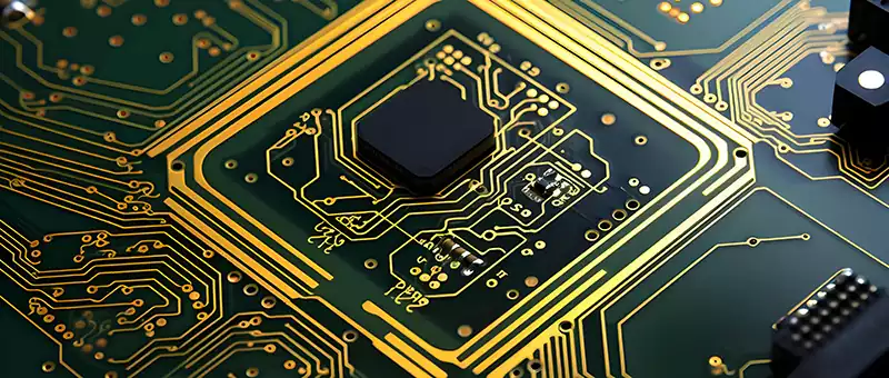
In the present era of rapid and unprecedented advancements in artificial intelligence technology, AI servers have emerged as the pivotal infrastructure underpinning computational power, their significance growing ever more pronounced. High layer PCBs and flip-chip ball grid array (FC-BGA) substrates, serving as critical components within AI server PCBs, function akin to the heart and neural network of the server. They play a decisive role in determining the system’s performance, reliability, and integration level. However, the manufacturing processes for these two core components resemble scaling technological peaks, involving complex materials science, precision machining techniques, and challenging process control issues. These have become critical bottlenecks hindering further performance enhancements in AI servers.
- High layer PCB: The Tough Balancing Act Between High-Density Interconnection and Ultra-Thick Board Processing
The Core Mission of High Layer PCBs in AI Servers
High layer PCBs, typically referring to PCB boards with 20 or more layers, undertake multiple core tasks within AI servers. They function as the internal traffic hub of the server, bearing the critical responsibility of high-speed signal transmission to ensure data flows rapidly and accurately between components. Simultaneously, they provide stable pathways for high-power supply, guaranteeing all server components receive adequate energy support. Furthermore, high-layer PCBs enable the integration of complex circuits, connecting numerous electronic components in an orderly fashion to form an efficiently operating whole. As AI chip computing power exhibits exponential growth, demands on PCB performance have risen accordingly, pushing layer counts beyond previous limits—now exceeding 40 layers and beyond. However, increased layer counts introduce new challenges, with the tension between interlayer interconnect density and signal integrity becoming increasingly acute. Much like traffic congestion, this hinders the smooth transmission of data.
Through-Hole Processing: Dual Bottlenecks of Material and Process
To meet high-speed signal transmission demands, high layer PCBs predominantly utilise M6 or M7 grade high-frequency, high-speed substrates. These materials possess unique characteristics, notably high glass fibre content, which lowers their dielectric constant and facilitates rapid signal propagation. However, this high glass fibre content also introduces significant drawbacks: markedly increased material hardness and brittleness, posing substantial processing challenges. In the through-hole drilling stage, micro-apertures below 0.2mm are increasingly becoming the mainstream requirement to achieve higher integration and finer circuit layouts. Yet, ultra-fine drill bits (such as those with a diameter of 0.1mm) face numerous difficulties when machining these minute apertures. Due to the extremely small diameter of the drill bit, heat dissipation efficiency becomes extremely low. The heat generated during machining is difficult to dissipate rapidly, causing the drill bit temperature to rise sharply. Concurrently, the chip evacuation pathway becomes extremely narrow, hindering the smooth removal of machining debris and increasing the likelihood of blockages within the hole. The intense friction between the drill and the material can cause the hole wall roughness (Ra value) to exceed the critical threshold of 1.6μm. This is akin to placing obstacles on a smooth road, triggering signal reflection and impedance mismatch, which in turn compromises signal transmission quality. Furthermore, for extremely thick boards (1.6–4.0mm), multi-layer stacked drilling is required. This process involves several times the material removal of conventional PCB boards, significantly shortening drill bit lifespan by over 30% due to prolonged high-intensity operation. This creates a pronounced conflict between production capacity pressures and cost control. Enterprises face a dilemma: they must ensure production efficiency to meet market demand while simultaneously controlling costs to maintain competitiveness.
High-Drill Compensation and the Stub Effect: The Art of Balance
To enhance signal transmission rates, back drilling technology is widely employed in the manufacture of high-layer-count boards. The core objective of this technique is to eliminate residual copper stubs within vias, as these stubs act as speed bumps on the signal transmission path, impeding rapid signal propagation and causing signal reflection and loss. However, when drilling depth compensation reaches D + 6 mil (approximately 0.15 mm), traditional CCD full-board compensation systems prove inadequate. Due to misalignment between mixed holes and via centres (typically ±25 μm), conventional systems cannot compensate accurately, resulting in suboptimal compensation. More critically, board thickness variation poses significant challenges to back drilling. For instance, the lamination tolerance for a 2.3mm substrate is ±5%, implying thickness variations within a defined range. Such thickness variations directly cause stub lengths to fluctuate randomly between 2 and 8 mils. This instability, akin to uneven speed bumps on a signal transmission pathway, induces phase noise in high-frequency signals. Particularly in SerDes channels exceeding 112Gbps, this phase noise can trigger a sharp rise in bit error rate (BER), severely compromising data accuracy and posing potential risks to server stability.
Interlayer Alignment and Thermal Stress Management: Pursuing Precision and Stability
High layer pcbs demand exceptionally high interlayer alignment accuracy, requiring control within ±50μm to ensure precise circuit connection between layers and enable normal signal transmission. However, during high-temperature lamination, the differing coefficients of thermal expansion (CTE) between materials present a significant obstacle to achieving this alignment. For instance, copper foil exhibits a CTE of approximately 17 ppm/°C, whereas resin has a CTE of around 50 ppm/°C. At lamination temperatures (180–200°C), the expansion disparity between these materials can reach 0.1%. For PCB boards exceeding 40 layers, this minute expansion differential accumulates, posing a direct threat to yield rates. Consider a multilayer circuit board akin to a skyscraper: if each layer exhibits minute positional deviations, the entire structure’s stability is compromised. To address this, the industry has adopted low-CTE resin systems and laser direct imaging (LDI) technology. Low-CTE resin systems minimise material expansion during temperature fluctuations, while laser direct imaging compensates for thermal distortion through precise exposure. This enhances interlayer alignment accuracy, safeguarding PCB board quality.
- FC-BGA Substrates: Pushing the Limits of Micrometre-Level Precision
The Critical Role of FC-BGA Substrates in AI Servers
FC-BGA substrates serve as the vital intermediary layer between AI chips and PCB boards, playing an indispensable role. Functioning as a bridge connecting the chip and PCB, their primary purpose is to enable high-density I/O interconnections and thermal management. As chip fabrication processes advance towards ever-smaller dimensions—now entering the 3nm era—demands on substrate performance intensify. Substrate routing density has surpassed 200 lines/mm², with line width/spacing (L/S) reduced below 8/8μm. This imposes near-impossible requirements on substrate manufacturing, akin to constructing a complex city within minute spaces where every detail demands flawless precision.
Resin Viscosity and Drilling Processes: Resolving the Conflict
FC-BGA substrates commonly employ BT resin or ABF materials with high glass transition temperatures (Tg > 200°C). These materials offer numerous advantages, enhancing the reliability of chip packaging. The elevated glass transition temperature ensures the material maintains stable performance under high temperatures, resisting deformation and thereby safeguarding normal chip operation. However, these materials present drawbacks: their high viscosity and toughness result in extremely inefficient chip removal during drilling. When processing micro-holes (diameter < 0.1mm), debris readily accumulates within the bore. If not promptly evacuated, friction-generated heat causes carbonisation, forming irreversible wall defects. Such defects, akin to impurities within precision instruments, compromise the entire system’s performance. To address this, drill bits require special coatings (such as diamond-like carbon films) to reduce friction coefficients, minimising chip generation and accumulation. Concurrently, vacuum-assisted chip evacuation systems are employed to promptly remove debris from the bore. Nevertheless, these enhancements introduce new challenges: single-hole processing costs increase by over 40%, placing enterprises under dual pressure to pursue high quality while managing expenditure.
Interconnect Density and Drilling Precision: Strategies for Resolving Process Conflicts
Amidst escalating wiring density requirements, substrate drilling positional accuracy must achieve ±15μm (CPK≥1.33). This necessitates positioning systems with repeatability exceeding ±5μm. Traditional mechanical drilling machines, however, suffer from spindle thermal expansion, introducing temperature drift of ±3μm/℃ during continuous operation. This effect resembles the minute barrel deflection in firearms caused by temperature variations, adversely impacting drilling precision. To meet precision requirements, conventional mechanical drilling machines must operate within temperature-controlled workshops (±0.5℃) to minimise thermal variations’ impact on machining accuracy. More critically, individual carrier boards now feature over 500,000 holes, extending processing times beyond 20 hours. During prolonged machining, cumulative taper caused by drill bit wear can reach ±8μm – akin to dimensional deviations in engraving due to tool abrasion over extended periods. Addressing this requires dynamic compensation algorithms to adjust feed rates in real-time, automatically modifying parameters based on drill bit wear to maintain drilling precision.
Microvia Metallisation and Signal Loss: Breakthrough Directions in the Trade-off Dilemma
To achieve low-loss transmission of high-frequency signals, the uniformity of copper plating in carrier board microvias must be controlled within ±3μm. However, when aperture sizes shrink below 0.05mm, the fluidity of the plating solution diminishes. Much like water flowing poorly through a narrow channel, this exacerbates uneven copper thickness distribution within the vias. While pulse plating and additive optimisation can enhance deep plating capability and improve copper layer uniformity, these methods introduce organic impurities, causing dielectric loss (Df value) to rise above 0.005. This contradiction becomes particularly pronounced in the 112GHz millimetre-wave band, as this frequency range is highly sensitive to signal loss, where even minute variations in loss can compromise transmission quality. To overcome this bottleneck, synergistic innovation in both materials (such as modified polyimides) and processes (such as ALD atomic layer deposition) is required. Modified polyimide materials exhibit superior electrical properties that reduce dielectric loss, while ALD enables high-precision thin-film deposition to enhance copper plating uniformity. This approach ensures low-loss signal transmission while meeting routing density requirements.
- Small Module PCBs: The Emergence of High-Precision Forming Demands
Application Trends of Small Module PCBs in AI Servers
Modular design in AI servers represents a prevailing development trend, offering advantages such as simplified maintenance, upgrades, and scalability. With the proliferation of modular architecture, demand for miniaturised PCBs—including optical modules and HBM memory modules—has surged exponentially. These compact PCB boards function as critical components within servers, performing complex operations within constrained spaces and thus demanding exceptionally high forming precision.
Technical Challenges and Solutions for High-Precision Forming
During forming, these boards require hole-to-edge alignment accuracy within ±35μm. However, the ±80μm tolerance of traditional mechanical forming machines falls short of this requirement—akin to attempting precise measurements of minute objects with a coarse ruler. To resolve this, CCD optical forming machines emerged. Equipped with high-resolution cameras (5μm pixel resolution), they capture positioning markers in real time – akin to granting the forming machine “eagle eyes” – enabling precise identification of positional data on the board. By integrating motion control algorithms for dynamic tool path compensation, the system adjusts the cutting trajectory in real-time based on captured positional data, elevating precision to ±15μm. This technology, however, demands exceptionally stringent requirements for vibration suppression, light source stability, and algorithmic latency (necessitating <1ms response). Vibration acts as an external interference factor, affecting both camera imaging precision and tool movement stability. Insufficient light source stability leads to blurred images, compromising positioning accuracy. Excessive algorithm latency prevents timely tool path adjustments, resulting in diminished machining precision. Consequently, the equipment cost of CCD optical moulding machines is 3–5 times that of traditional solutions, requiring enterprises to balance cost considerations while pursuing high precision.
- Future Technological Trends: Convergence of Materials, Processes and Intelligence
Material Innovation: The Key to Overcoming Physical Limitations
Faced with the extreme demands of AI servers on PCB board performance, material innovation is pivotal to transcending physical constraints. Developing composite substrates with low CTE and low loss characteristics—such as carbon fibre-reinforced resins—represents a crucial future direction. Carbon fibre-reinforced resins exhibit outstanding mechanical and electrical properties. Their low CTE reduces thermal expansion during temperature fluctuations, enhancing interlayer alignment precision; low loss minimises energy dissipation during signal transmission, improving signal integrity. Additionally, exploring interlayer technologies based on silicon substrates holds significant promise. Silicon substrates possess excellent electrical properties and thermal stability, offering potential to overcome the physical limitations of traditional organic materials and provide robust support for AI server development.
Process Upgrades: Advancing Towards Greater Precision and Efficiency
Process upgrades represent a vital pathway to enhancing PCB manufacturing quality and efficiency. Laser drilling will progressively replace mechanical drilling, with picosecond lasers offering distinct advantages. Their extremely short pulse duration enables 5μm aperture processing while avoiding heat-affected zones (HAZ), akin to carving with an exceptionally sharp and precise blade. This approach prevents thermal damage to surrounding materials, thereby elevating processing accuracy and quality. Furthermore, AI-based real-time defect detection systems will become a vital safeguard in future PCB manufacturing. By analysing diverse process data, these systems can anticipate processing anomalies, promptly identify potential issues, and issue alerts. This elevates yield rates to over 99.5%, reduces scrap rates, and boosts production efficiency.
Equipment Intelligence: Achieving ‘Zero-Defect’ Manufacturing
Equipment intelligence represents the future trajectory of PCB manufacturing. Digital twin technology simulates processing parameters, enabling comprehensive virtual simulation and analysis of the manufacturing process. This allows for the early identification of potential issues and optimisation of processing parameters, akin to conducting a full-scale rehearsal prior to actual production. Combined with edge computing to optimise drill bit lifespan and energy consumption, edge computing enables real-time data processing and analysis at the equipment level. It automatically adjusts drill bit usage parameters based on processing conditions, extending bit lifespan and reducing energy consumption. Achieving ‘zero-defect’ manufacturing represents the ultimate goal for future PCB production. Through the integrated advancement of materials, processes, and intelligent systems, this objective can be progressively approached, providing more reliable support for AI server development.
Technological breakthroughs in high layer pcbs and FC-BGA carrier boards form the foundation for AI servers advancing towards higher computing power and energy efficiency ratios. From microscopic explorations in materials science to macro-level strategic planning in intelligent manufacturing, every optimisation of process details embodies the ingenuity and innovation of engineers. Within materials science, researchers continually explore novel material systems, seeking materials with superior properties; In the realm of intelligent manufacturing, engineers dedicate themselves to developing more advanced processing equipment and techniques, enhancing production efficiency and product quality. Looking ahead, with the convergence of technologies such as 5G and quantum computing, PCB manufacturing will evolve beyond being merely an arena for precision processing; it will become a frontier for multidisciplinary integration. Only by persistently pushing the boundaries of physical limitations and redefining manufacturing paradigms can we meet the boundless computational demands of the AI era, propel the continuous advancement of artificial intelligence technology, and bring greater benefits to human society.