Electronic packaging ceramic substrates, leveraging their unique advantages amidst the sweeping tide of continuous innovation in semiconductor technology, occupy a pivotal position in the advancement of power devices. Presently, power devices—particularly third-generation semiconductors—are rapidly emerging and finding widespread application, propelling the entire semiconductor device sector towards high power, miniaturisation, integration, and multifunctionality.
This pronounced developmental trajectory imposes exceptionally stringent and unprecedented demands upon packaging substrate performance. Ceramic substrates for electronic packaging stand as the pivotal supporting force fulfilling these requirements and propelling the advancement of power devices.
The evolution of semiconductor technology resembles an epic technological saga, having traversed three generations of landmark transformations throughout history.
The first generation of semiconductors, typified by silicon (Si) and germanium (Ge), served as the solid foundation of the electronic world, excelling in data processing. It laid the bedrock for the burgeoning microelectronics industry, successfully ushering in the digital age. Computers and other electronic devices thus entered ordinary households, fundamentally reshaping how people lived and worked, ushering human society into a new era of informatisation. Throughout this process, while electronic packaging ceramic substrates remained largely unnoticed, they quietly provided foundational support in the device encapsulation stage, ensuring the stable operation of first-generation semiconductor components.
With communications technology advancing at rocket speed, second-generation semiconductors emerged. Represented by gallium arsenide (GaAs) and indium phosphide (InP), these materials shifted the focus to the communications sector, becoming core components for manufacturing high-performance microwave, millimetre-wave, and light-emitting devices. These materials provided powerful wings for the take-off of the information industry, making high-speed, stable communications a reality. They vigorously propelled the rapid development of fields such as the internet and mobile communications, rendering global information exchange more convenient and efficient than ever before. At this juncture, electronic packaging ceramic substrates assumed an increasingly vital role in the encapsulation of second-generation semiconductor devices. Their outstanding properties, such as excellent insulation and high thermal conductivity, better meet the packaging environment requirements of second-generation semiconductor devices. This ensures stable operation in complex communication settings, further bolstering the prosperity of the information industry.
However, technological advancement never ceases. As techniques continue to progress and application demands expand, the limitations of the first two generations of semiconductors gradually became apparent. They struggle to meet the growing demands for high frequency, high temperature, high power, high energy efficiency, resistance to harsh environments, portability, and miniaturisation. Against this backdrop, third-generation semiconductor materials, represented by silicon carbide (SiC) and gallium nitride (GaN), have emerged as the shining new stars in the semiconductor field. Third-generation semiconductor materials possess exceptional properties including wide bandgap, high critical breakdown voltage, high thermal conductivity, and high carrier saturation drift velocity. These characteristics enable electronic devices manufactured from them to operate stably at temperatures of 300°C or higher, hence their designation as power semiconductors or high-temperature semiconductors.
Electronic packaging ceramic substrates face unprecedented opportunities and challenges amidst the development wave of third-generation semiconductors. Electronic devices manufactured using third-generation semiconductors—such as solid-state light sources (e.g., LEDs), lasers (LDs), power electronics (e.g., IGBTs), concentrated photovoltaics (CPV), and microwave radio frequency (RF) components—impose increasingly stringent demands on packaging substrates. Ceramic substrates for electronic packaging, however, emerge as the ideal choice for these third-generation semiconductor devices due to their unique advantages. Not only can they withstand the high thermal loads generated by third-generation semiconductor devices, enabling efficient heat dissipation and ensuring stable performance under high-temperature conditions, but they also possess excellent electrical properties that meet the signal transmission and insulation requirements of these devices. In numerous fields including semiconductor lighting, automotive electronics, next-generation mobile communications (5G), new energy and new energy vehicles, high-speed rail transport, and consumer electronics, electronic packaging ceramic substrates work in close synergy with third-generation semiconductors, demonstrating broad application prospects. It holds promise in overcoming the limitations of traditional semiconductor technology, delivering significant application value in optoelectronic devices, power electronics, automotive electronics, aerospace, deep well drilling, and other sectors. This will inject powerful momentum into energy conservation, emissions reduction, industrial transformation and upgrading, and the cultivation of new economic growth points, propelling semiconductor technology towards an even more brilliant future.
Thermal Management Challenges in Power Device Development and the Critical Role of Packaging Substrates
With the continuous advancement of power devices (including LEDs, LDs, IGBTs, CPVs, etc.), thermal management has emerged as a critical technical bottleneck affecting device performance and reliability. The effective lifespan of electronic components is closely correlated with temperature; typically, every 10°C increase reduces effective lifespan by 30%–50%. Taking high-power LED packaging as an example, 70%–80% of the input power is converted into heat, with only approximately 20%–30% transformed into light energy. Moreover, the small chip area and high power density exceeding 100W/cm² make thermal management particularly critical. If the heat generated by the chip cannot be dissipated promptly, substantial thermal energy accumulates within the LED, causing the junction temperature to rise progressively. This not only degrades LED performance—such as reduced luminous efficacy and wavelength red-shift—but also generates thermal stresses within the device, triggering reliability issues including shortened lifespan and colour temperature shifts.
The packaging substrate plays a critical role in thermal management for power devices, primarily leveraging its high thermal conductivity to conduct heat away from the chip (heat source) and facilitate heat exchange with the external environment. For power semiconductor devices, the packaging substrate must meet a series of stringent requirements:
High Thermal Conductivity
Currently, power semiconductor devices predominantly employ thermo-electrically decoupled packaging. The majority of heat generated by the device is transmitted through the packaging substrate. Consequently, a substrate with excellent thermal conductivity can rapidly dissipate heat, effectively protecting the chip from thermal damage and ensuring the device’s stability and reliability during prolonged high-power operation.
Thermal expansion coefficient matching the chip material
Although power device chips possess high-temperature resistance, variations in current, environment, and operating conditions cause their temperature to fluctuate. As the chip is directly mounted on the packaging substrate, mismatched thermal expansion coefficients between the two materials generate thermal stresses during temperature changes. These stresses may lead to issues such as loosening or cracking of the chip-to-substrate bond, severely compromising device reliability. Therefore, the thermal expansion coefficient of the packaging substrate must match that of the chip material to minimise thermal stress and enhance overall device reliability.
Excellent heat resistance, meeting high-temperature requirements with superior thermal stability
Power devices often generate significant heat during operation. The packaging substrate must possess excellent heat resistance, maintaining stable performance under high temperatures without deformation, softening, or decomposition, thereby ensuring normal device operation in high-temperature conditions.
Excellent insulation
Meeting electrical interconnection and equipment insulation requirements is a key function of packaging substrates. Superior insulation prevents current leakage, avoids electrical faults such as short circuits, and safeguards the secure operation of devices and equipment.
High mechanical strength
During device processing, packaging, and application, substrates endure various mechanical stresses including pressure, vibration, and impact. Therefore, substrates must possess sufficient mechanical strength to withstand these external forces without damage, ensuring stability and reliability throughout all stages of device operation.
Cost-Effectiveness for Mass Production Applications
While pursuing high performance, the cost of packaging substrates significantly influences their widespread adoption. Only when priced reasonably and capable of meeting mass production demands can they achieve broad market penetration and application, thereby accelerating the rapid development of the power device industry.
Characteristics and Advantages of Ceramic Substrates for Electronic Packaging
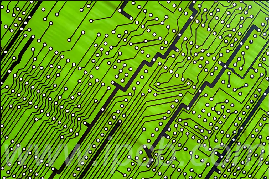
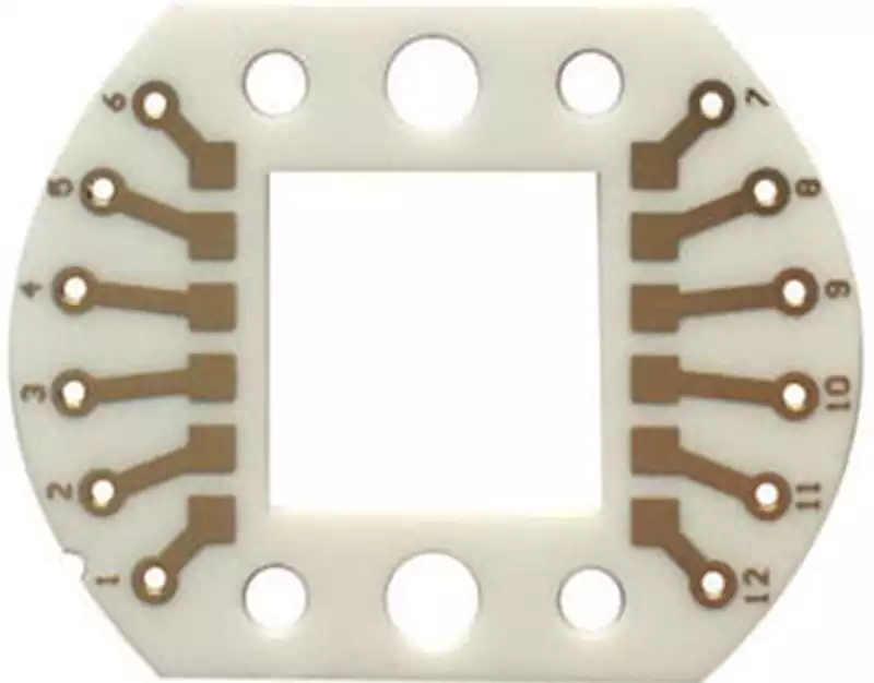
Ceramic substrates for electronic packaging (also known as ceramic circuit boards) represent an ideal solution for meeting the aforementioned packaging substrate requirements due to their unique physical and chemical properties. They offer numerous advantages including high thermal conductivity, excellent heat resistance, low thermal expansion coefficient, high mechanical strength, insulation, corrosion resistance, and radiation resistance.
Physical Properties of Common Ceramic Substrate Materials
Commonly used ceramic substrate materials include aluminium oxide (Al₂O₃), aluminium nitride (AlN), silicon nitride (Si₃N₄), beryllium oxide (BeO), silicon carbide (SiC), and boron nitride (BN). Aluminium oxide ceramic substrates offer excellent electrical insulation, mechanical strength, and chemical stability at a relatively low cost, making them one of the most widely used ceramic substrate materials today. However, their thermal conductivity is comparatively low, typically around 20–30 W/(m·K), which limits their application in high-power devices to some extent. Aluminium nitride ceramic substrates exhibit high thermal conductivity, reaching 170–230 W/(m·K), alongside excellent insulation and heat resistance. Their thermal expansion coefficient is well-matched to silicon chips, making them a superior ceramic substrate material, though at a relatively higher cost. Silicon nitride ceramic substrates exhibit thermal conductivity of approximately 80–100 W/(m·K), coupled with high mechanical strength, excellent thermal resistance, and thermal shock resistance, making them suitable for high-temperature, high-stress operating environments. Beryllium oxide ceramic substrates possess exceptionally high thermal conductivity, reaching 330 W/(m·K), though their significant toxicity imposes certain application limitations. Silicon carbide ceramic substrates combine high thermal conductivity with exceptional hardness, wear resistance, and chemical stability, making them suitable for power device packaging in harsh environments. Boron nitride ceramic substrates offer outstanding thermal conductivity and electrical insulation alongside good chemical stability, though they are comparatively expensive.
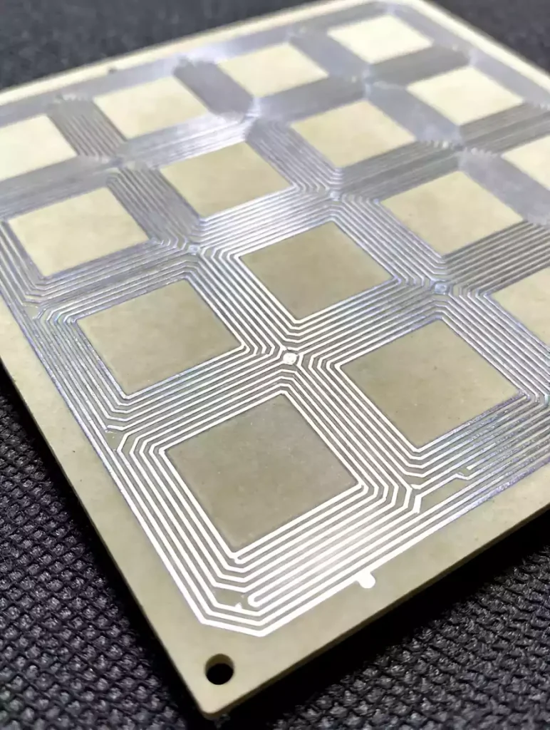
Principles, Process Flows, and Technical Characteristics of Various Ceramic Substrate Preparations
Currently, common ceramic substrate preparation technologies include thick-film ceramic substrates (TFC), thin-film ceramic substrates (TPC), direct-bonded copper ceramic substrates (DBC), direct-plated copper ceramic substrates (DPC), active metal brazed ceramic substrates (AMB), laser-activated metallised ceramic substrates (LAM), and various 3D ceramic substrates. Each preparation technique possesses distinct principles, process flows, and technical characteristics. For instance, DBC technology involves direct copper plating onto the ceramic substrate surface, followed by high-temperature eutectic reaction to achieve robust copper-ceramic bonding. It offers advantages such as simplified processes, lower costs, and high bonding strength, finding extensive application in power electronics. DPC technology employs thin-film processes such as photolithography and electroplating to fabricate metallic circuits on ceramic substrates. It offers high circuit precision and enables microfabrication, making it suitable for high-frequency, high-density electronic device packaging. AMB technology utilises active metal solders to connect ceramics and metals, providing high bonding strength and excellent reliability. It is frequently employed in sectors demanding exceptional reliability, such as aerospace.
Electronic packaging ceramic substrates, with their outstanding performance and diverse fabrication techniques, provide robust support for power device development. As third-generation semiconductor technology advances and application domains expand, these substrates will encounter broader development prospects. They are poised to play an increasingly vital role in driving power devices towards higher performance, smaller dimensions, and lower costs, thereby propelling the electronics industry to new heights.