With the continuous increase in power density and operating frequency of electronic systems, traditional organic PCB materials are gradually reaching their performance limits. Ceramic PCBs, characterized by high thermal conductivity, excellent dimensional stability, and superior dielectric performance, have become an important solution for high-power, high-frequency, and high-reliability applications.
However, compared with conventional FR-4 PCBs, ceramic substrates exhibit fundamentally different material properties, which impose stricter requirements on routing design. Therefore, effective routing on ceramic PCBs is not merely a matter of trace placement, but a systematic engineering task involving electrical performance, thermal behavior, and manufacturability.
Characteristics of Ceramic PCB Substrates and Their Impact on Routing
Ceramic PCB substrates are typically based on alumina (Al₂O₃), aluminum nitride (AlN), or silicon nitride (Si₃N₄). These materials feature significantly higher thermal conductivity and elastic modulus than organic laminates, while their coefficient of thermal expansion is much closer to that of semiconductor devices.
As a result, ceramic PCBs exhibit minimal deformation under thermal cycling. However, due to their rigidity and brittleness, routing errors such as sharp corners, excessive copper density concentration, or abrupt width transitions may introduce localized stress, which can lead to microcracks in both conductors and substrate.
Therefore, routing on ceramic PCBs must prioritize mechanical stress distribution while maintaining electrical performance.
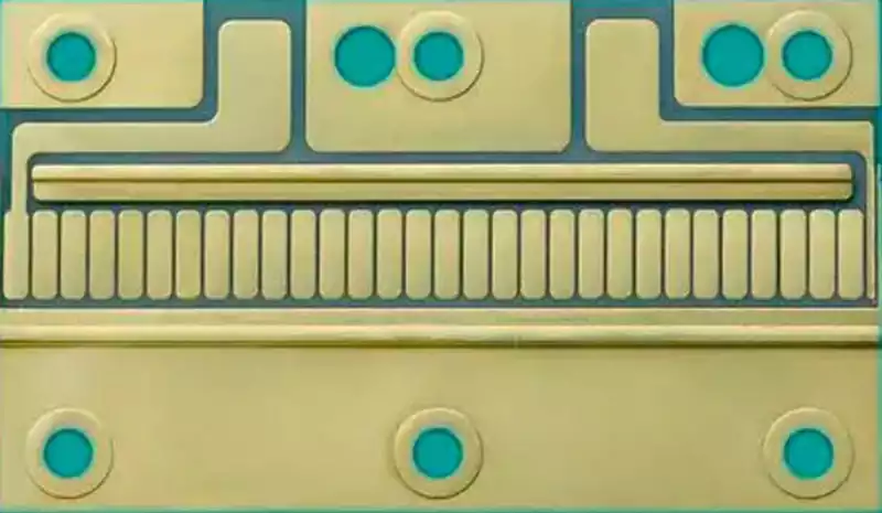
Trace Width, Spacing, and Geometry Control
In ceramic PCB design, trace width and spacing are directly constrained by the manufacturing process, which typically includes thick-film printing, thin-film deposition, or direct copper bonding (DBC).
Under controlled ceramic PCB processes, trace widths can be accurately maintained, but excessive narrowing of traces may increase current density and localized heating. At the same time, insufficient spacing between adjacent conductors may cause insulation reliability risks, especially under high-voltage or high-humidity operating conditions.
To mitigate these risks, routing should adopt smooth and uniform trace geometries. Acute angles should be avoided, and 45-degree or curved routing is recommended to reduce electric field concentration and mechanical stress accumulation.
Impedance Control and Signal Integrity Considerations
Due to the relatively stable dielectric constant of ceramic materials, impedance predictability on ceramic PCBs is inherently superior to that of organic substrates. However, this advantage can only be fully realized if routing parameters are strictly controlled.
In high-speed or high-frequency applications, trace impedance is determined by conductor width, copper thickness, dielectric thickness, and reference plane configuration. Since ceramic substrates typically allow thinner dielectric layers, small variations in routing dimensions may result in noticeable impedance deviation.
Therefore, impedance-controlled traces should be routed with consistent width and reference structure throughout their entire length. Any abrupt transition, such as neck-downs or unnecessary via transitions, should be minimized to ensure signal integrity and repeatability.
Thermal-Aware Routing Strategy
One of the primary advantages of ceramic PCBs lies in their excellent heat dissipation capability. However, improper routing may limit the effectiveness of thermal conduction paths.
High-current or high-power traces should be designed with sufficient width to reduce resistive losses, and they should be routed to facilitate direct heat spreading into the ceramic substrate. In addition, copper distribution should be balanced to avoid localized hot spots, which may otherwise lead to uneven thermal expansion and mechanical stress.
When possible, power and ground routing should be implemented as large-area copper regions rather than narrow traces, thereby maximizing both electrical performance and thermal conduction efficiency.
Via Design and Interconnection Routing
Compared with organic PCBs, vias in ceramic PCBs are more limited in size, quantity, and placement due to processing constraints. Improper via design may significantly increase manufacturing complexity and cost.
As a result, routing should aim to minimize unnecessary layer transitions. Signal paths should be kept as direct as possible, and via usage should be carefully evaluated based on electrical necessity rather than layout convenience.
For high-reliability applications, redundant vias or oversized vias should be avoided, as they may introduce stress concentration points within the ceramic substrate.
Design for Manufacturability (DFM) Considerations
Effective routing on ceramic PCBs must align closely with the selected manufacturing process. Different ceramic PCB technologies impose different minimum line widths, spacing rules, and copper thickness limitations.
Therefore, routing rules should be defined early in the design phase in collaboration with the PCB manufacturer. By doing so, potential yield risks such as line breakage, incomplete metallization, or pattern distortion can be identified and mitigated before fabrication.
A routing design that strictly adheres to process capabilities not only improves manufacturing yield but also ensures long-term reliability of the final product.
Effective routing on ceramic PCBs is a multidisciplinary optimization process that integrates electrical design, thermal management, mechanical reliability, and manufacturing constraints. Compared with conventional PCBs, ceramic substrates provide superior performance potential, but only when routing strategies are carefully tailored to their unique material characteristics.
By implementing controlled trace geometry, impedance-consistent routing, thermal-aware copper distribution, and process-aligned design rules, ceramic PCBs can achieve high circuit density, stable electrical performance, and long-term operational reliability. These advantages make ceramic PCBs a critical foundation for next-generation power electronics, RF modules, and high-reliability industrial applications.