In the wave of nanotechnology, two-dimensional materials have become a focus in the field of materials science due to their atomic scale thickness and unique physical properties. Among them, High-k 2D materials are gradually becoming a key force driving the innovation of electronic devices due to their excellent electrical properties and broad application prospects. Compared to traditional dielectric materials such as silicon oxide and stereoscopic high-k materials, high-k two-dimensional materials exhibit significant advantages, providing the possibility to break through technological bottlenecks and meet emerging demands
1、 Definition and Characteristics of High Dielectric Constant Two Dimensional Materials
The dielectric constant (k) is an indicator of a material’s ability to store charges in an electric field. High dielectric constant materials typically refer to materials with a dielectric constant much higher than that of silicon oxide (SiO ₂, k ≈ 3.9), while high-k two-dimensional materials combine high dielectric properties with the advantages of two-dimensional structures, with a thickness of only a single or a few atomic layers. These materials not only achieve high capacitance density with ultra-thin structures, but also retain the unique atomic level flat surface, high mechanical strength, and flexibility of two-dimensional materials.
2、 The main characteristics of high-k two-dimensional materials include:
Ultra high dielectric constant: up to 15-100 or more, significantly reducing equivalent oxide thickness (EOT) and improving capacitance density.
Atomic level thickness: thickness as low as 0.5-1 nm, suitable for nanoscale devices.
Excellent interface quality: Atomic level flat surface reduces charge scattering and defects, improving device performance.
High stability: It exhibits stability in high temperatures or complex chemical environments.
Flexibility and mechanical strength: Supports flexible electronic applications and can withstand bending and stretching.
High thermal conductivity: Some materials (such as h-BN) have excellent heat dissipation capabilities, improving device thermal management.
3、 Representative high-k two-dimensional materials
There are a wide variety of high-k two-dimensional materials, each of which exhibits unique advantages in a specific field. Here are several “star” representatives:
Perovskite two-dimensional materials
Perovskite structured materials (such as SrTiO3, BaTiO3) can have a dielectric constant exceeding 100, and can be prepared in single or few layer form through exfoliation technology. They are suitable for high-density capacitors and sensors and can be regarded as a “heavyweight player” in the field of high-k
Two dimensional hafnium oxide (HfO ₂)
Hafnium oxide is a two-dimensional extension of traditional high-k materials, with a dielectric constant of 15-25 and excellent thermal and chemical stability. Two dimensional HfO ₂ prepared by exfoliation or chemical vapor deposition (CVD) exhibits excellent performance in ultra-thin transistors and memory devices.
Hexagonal boron nitride (h-BN) composite material
H-BN itself has a low dielectric constant (k ≈ 4), but by combining with high-k oxides (such as HfO ₂), its performance can be greatly improved while maintaining excellent insulation and high thermal conductivity, making it highly promising in high-frequency devices and quantum computing.
Modified transition metal disulfide
Materials such as molybdenum disulfide (MoS ₂) can increase their dielectric constant through surface oxidation or doping, while retaining flexibility and transparency, making them suitable for flexible electronics and wearable devices.
4、 High dielectric constant polymer type
Ceramic filled polymer dielectric
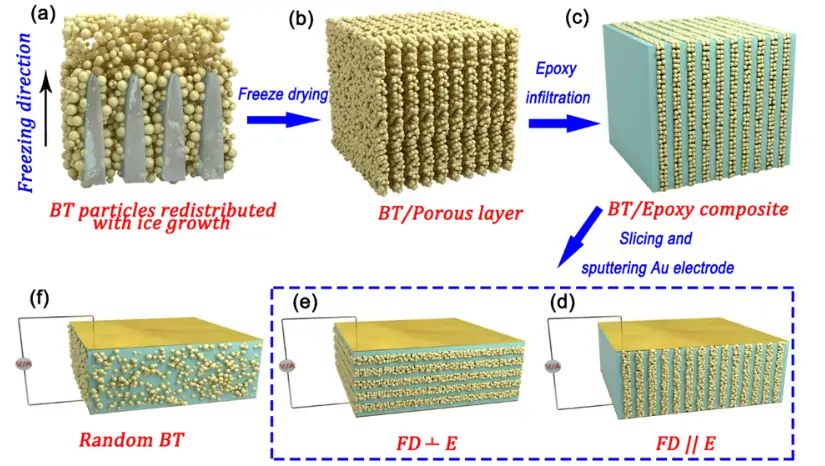
Adding ferroelectric ceramic powders with high dielectric constant, such as barium titanate, strontium barium titanate, etc., to the polymer matrix is the earliest and main method for obtaining high dielectric constant polymers. Although ceramic filled polymer composite dielectrics can combine the characteristics of high dielectric constant of ceramics and low loss of polymers, the enhancement effect on the dielectric constant of composite materials is still limited (ε<100) at higher ceramic powder filling amounts (>50wt%). Fillers also lead to difficulties in processing such materials and a decrease in mechanical strength. In addition, due to the nanoscale effect, the ferroelectric properties of ceramic particles disappear when they are less than 100 nanometers, which further limits the development of high dielectric thin film materials smaller than micrometers and severely restricts the widespread application of ceramic/polymer dielectric materials.
Conductive filler filled polymer dielectric
Adding some conductive fillers such as metal powder, carbon black, carbon nanotubes, and graphite to the polymer causes a sudden change in the dielectric properties of the composite material near the percolation threshold (f). Especially when adding carbon nanotubes and graphene materials with high aspect ratios, a small amount of filler can obtain dielectrics with high dielectric constants, while maintaining the good toughness and mechanical strength of the polymer itself. However, the biggest drawback of the infiltration system is that conductive pathways are easily formed between the fillers in the vicinity, resulting in significant dielectric loss of the material and seriously affecting the service life and safety of the dielectric
Ternary or multivariate hybrid systems
Simple binary composite systems have performance bottlenecks, as dielectrics often suffer from high filling or loss issues while achieving high dielectric constants. In addition, binary systems are significantly affected by external fields and their dielectric properties are unstable. Researchers have integrated the advantages of traditional ceramic/polymer and conductive filler/polymer binary systems and explored many ternary or multicomponent hybrid systems. The ternary hybrid system has to some extent improved the drawbacks of traditional ceramic/polymer binary systems, and different fillers have played a significant synergistic enhancement role, with better comprehensive performance than traditional binary composite systems.
All organic polymer dielectric
In addition to the above-mentioned organic/inorganic composite dielectric materials, all organic dielectric materials are also an important research direction, mainly based on their better biocompatibility, which can be widely used in drug release, artificial muscles, and biochemical properties research.
Advantage
Improving device performance: In transistors, high dielectric constant materials can replace silicon dioxide (SiO ₂) as the gate dielectric, effectively reducing leakage current and improving device performance.
Flexibility and ease of processing (polymer based): Compared to inorganic ceramics, polymer based high dielectric materials have advantages such as lightweight, flexibility, and easy film-forming.
Improving capacitance: The capacitance is proportional to the dielectric constant, and high dielectric constant materials can significantly increase the capacitance of capacitors and achieve device miniaturization.
High energy storage density: In materials with high dielectric constant and high electrical breakdown strength, the energy storage efficiency is high.
Shortcoming
High temperature stability challenge: Some materials may experience changes in their performance (dielectric constant, loss) at high temperatures, which can affect the long-term stable operation of the device.
Difficult craftsmanship: Ceramic materials have high brittleness and high cost; Polymer composite materials need to optimize the dispersion and interface of fillers, otherwise it is easy to reduce the breakdown strength.
High dielectric loss: The introduction of highly polar groups or fillers can easily lead to molecular friction and charge accumulation at the interface, increasing energy loss in the form of thermal energy (dielectric loss, tan delta).
Challenge
Despite the enormous potential of high-k two-dimensional materials, they still face challenges such as large-scale preparation and the need to overcome cost and process bottlenecks for large-scale high-quality production. Interface defect: The interface between two-dimensional materials and electrodes needs further optimization. Stability: Some materials may degrade under high electric fields or high temperatures. Material diversity: More high-k two-dimensional materials need to be developed to meet diverse demands
application
Application
High dielectric constant polymers are commonly used to prepare capacitors and are widely used in energy and storage conversion devices such as audio and video equipment, industrial electronics and telecommunications equipment, automotive electronics, and various other pulse power devices. For capacitors, the stored electrical energy is proportional to the k value of the dielectric, which means that under other constant conditions, the use of high dielectric constant polymers can increase the capacity of capacitors and reduce their volume. Meanwhile, high dielectric constant polymers can be easily integrated onto curved substrates due to their excellent flexibility, chemical stability, biocompatibility, and other advantages, making them widely used in biological, fluid, and information storage applications, such as the preparation of wearable devices, biomedical sensors, wind turbines, and organic non-volatile storage devices
High dielectric constant two-dimensional materials are the electronic poetry of nanotechnology, carrying the dream of faster, smaller, and more intelligent devices with atomic level elegance. They have broken through the limitations of traditional dielectric materials, adapted to the rise of two-dimensional semiconductors, and illuminated the future of flexible electronics and quantum computing.