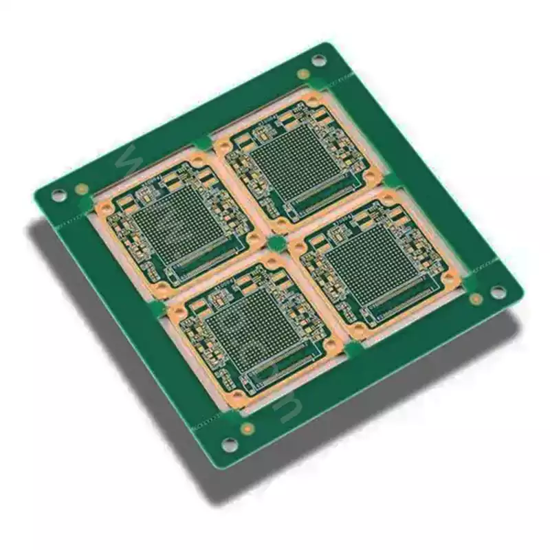
The high-density pin layout of BGA packaging is emerging as a core constraint on the path towards miniaturisation and high performance in premium electronic devices. When pin pitch shrinks to 0.5mm or even 0.4mm, traditional fan-out methods either suffer signal congestion due to insufficient routing space or experience performance degradation from excessively long bypass paths. The deep synergy between Via-in-Pad technology and High-Density Interconnect (HDI) processes offers the pivotal solution to overcome this challenge. Through precise structural design and process adaptation, these technologies enable efficient BGA pin fan-out within limited substrate space. This approach safeguards signal integrity while providing foundational support for slimmer end-product designs, making it widely applicable in high-performance scenarios such as ADAS radar, premium servers, and precision medical equipment.
As a core element in PCB design, BGA fan-out fundamentally involves extending the dense pins beneath the BGA package to other areas on the outer or inner layers of the substrate through rational routing, thereby establishing pathways for subsequent component connections and signal transmission. With soaring demands for integration in electronic devices, traditional fan-out solutions struggle to address three core challenges.
The conflict between pin density and available space is paramount. When BGA pin pitch shrinks from 1.0mm to below 0.5mm, routing channels between adjacent pins become less than 0.1mm wide. Traditional ‘dogbone’ fan-out methods require reserving via positions outside the pads, further encroaching on routing space. This prevents over 50% of pins from conventional fan-out, sometimes necessitating additional substrate layers that inflate costs and bulk. Signal integrity degradation is equally pronounced. Detour routing extends high-frequency signal transmission paths, readily inducing reflections and crosstalk. In high-frequency scenarios above 10GHz, signal attenuation can exceed 20%, severely compromising device performance. Furthermore, the separated via-pad design in traditional fan-out solutions is prone to poor contact under vibration or thermal cycling conditions, diminishing product reliability.
These challenges become more pronounced in high-end applications. Consider the high-precision millimetre-wave radar for ADAS systems: its core BGA package features pin pitches as narrow as 0.4mm, requiring simultaneous high-frequency and power signal fan-out. Traditional solutions struggle to balance density and performance. Similarly, high-end server CPUs with over a thousand pins demand fan-out efficiency that directly impacts data processing latency and stability. The synergistic solution combining Via-in-Pad and HDI technology addresses precisely these demands, achieving dual breakthroughs at both the structural and process levels.
The Synergistic Logic of Via-in-Pad and HDI
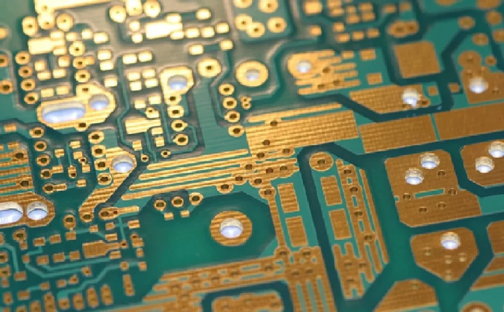
The core innovation of Via-in-Pad technology lies in fabricating vias directly within BGA pads rather than externally. This “via-pad integration” design liberates peripheral routing space entirely. Based on process variations, Via-in-Pad can be categorised into filled and unfilled types. The filled variant utilises materials such as resin or conductive paste to fill the vias. This approach prevents solder paste ingress during assembly, thereby avoiding cold solder joints, while also enhancing pad flatness and thermal dissipation. It represents the mainstream choice for high-performance applications.
HDI technology provides the critical foundation for implementing Via-in-Pad. Through techniques like laser via formation and buried/blind vias, HDI overcomes the limitations of conventional mechanical drilling. It enables micro-via processing down to 0.075mm – merely one-tenth the diameter of a human hair – while precisely controlling via positioning to ensure perfect alignment with BGA pads. Concurrently, HDI’s multi-layer routing capability enables 1st- to 3rd-order interconnect designs, or even higher-order configurations. This facilitates the layered transmission of signals routed via Via-in-Pad, further optimising routing density and signal paths.
The synergistic advantages manifest across three dimensions: In spatial efficiency, Via-in-Pad eliminates the footprint of vias around pads. Combined with HDI’s micro-via technology and multilayer routing, this increases routing density in BGA areas by over 35%. Signal performance: HDI’s short-path interconnections combined with Via-in-Pad’s integrated design reduce high-frequency signal transmission delay by 40%, controlling insertion loss within 1dB; In terms of reliability, HDI’s horizontal copper plating and pulse electroplating processes enhance via continuity stability. Combined with the structural reinforcement of the filled Via-in-Pad design, this ensures fault-free operation across temperature cycling from -40°C to 125°C and vibration environments spanning 10-2000Hz.
Optimising BGA fan-out through HDI process requires a tailored approach centred on three core dimensions: via geometry design, layer count planning, and routing rules. This must be combined with the characteristics of Via-in-Pad to formulate a customised solution balancing density, performance, and manufacturability.
Precise alignment of via geometry and filling processes forms the foundation. Select corresponding Via-in-Pad solutions for different signal types: high-frequency signals prioritise micro-via structures with resin filling and surface copper plating, maintaining a via diameter of 0.1-0.15mm precisely aligned with BGA pad centres to prevent signal reflection. Power signals may utilise larger-aperture Via-in-Pad filled with conductive paste to enhance current-carrying capacity. Concurrently, HDI laser drilling must match pad dimensions, ensuring contact area between hole walls and pads exceeds 60% of total pad area to mitigate connectivity failures. JLC’s practical data indicates that employing 0.1mm laser microvias with resin-filled Via-in-Pad elevates BGA fan-out yield from conventional 78% to over 95%.
HDI layer planning must dynamically align with BGA pin density. For medium-to-high density BGAs featuring 0.5mm pitch and 200-400 pins, efficient fan-out is achievable with 1-2 layer HDI: single-layer HDI directs signals via top/bottom laser vias to buried inner layer vias, then extends to outer layers; dual-layer HDI incorporates an intermediate interconnect layer to further compress routing space. For ultra-high-density BGAs with pitch below 0.4mm, such as CPU and FPGA packages, a third-level or higher HDI structure is required. This incorporates nested buried/blind vias to achieve layered fan-out for thousands of pins, reducing substrate area by 25%-30% compared to conventional solutions.
Optimising routing rules is central to ensuring signal integrity. Leveraging HDI’s multi-layer routing advantages, high-frequency signals, power signals, and ground signals must be layered separately. Via-in-Pad technology facilitates rapid interlayer switching, shortening signal paths. Maintain a minimum spacing of 0.3mm between adjacent Via-in-Pads to mitigate electromagnetic interference. Concurrently, implement impedance-matched design utilising low-loss HDI materials (e.g., S1000-2M) to suppress crosstalk in high-frequency signals above 5GHz to below -35dB. In a specific ADAS radar project, implementing this strategy elevated the signal integrity test pass rate in the BGA fan-out area from 82% to 98%, while reducing radar detection range error by 10%.
As electronic devices evolve towards higher frequencies and greater integration, the synergistic technology of Via-in-Pad and HDI continues to iterate. At the material level, development of HDI substrates with low dielectric loss and high thermal conductivity, coupled with novel filling materials, will further enhance high-frequency signal performance and heat dissipation capabilities, catering to emerging applications such as 6G communications and AI chips. Process-wise, automated laser micro-drilling technology will achieve precise control of apertures below 0.05mm. Concurrently, AI algorithms will optimise HDI layer counts and Via-in-Pad layouts, enhancing design efficiency and manufacturability. At the integration level, fusion with technologies like SiP and TSV will enable unified design of BGA packaging and substrates, constructing more compact and efficient interconnection systems.
The efficiency and quality of BGA fan-out directly determine the performance ceiling of high-end electronic devices. The synergistic solution of Via-in-Pad and HDI overcomes spatial constraints through structural innovation while safeguarding signal integrity via process upgrades, establishing itself as a core technological pillar in high-density interconnect. From laboratory breakthroughs to widespread mass production applications, this combination is propelling electronic devices towards greater thinness, efficiency, and reliability, empowering technological innovation and product upgrades across industries.