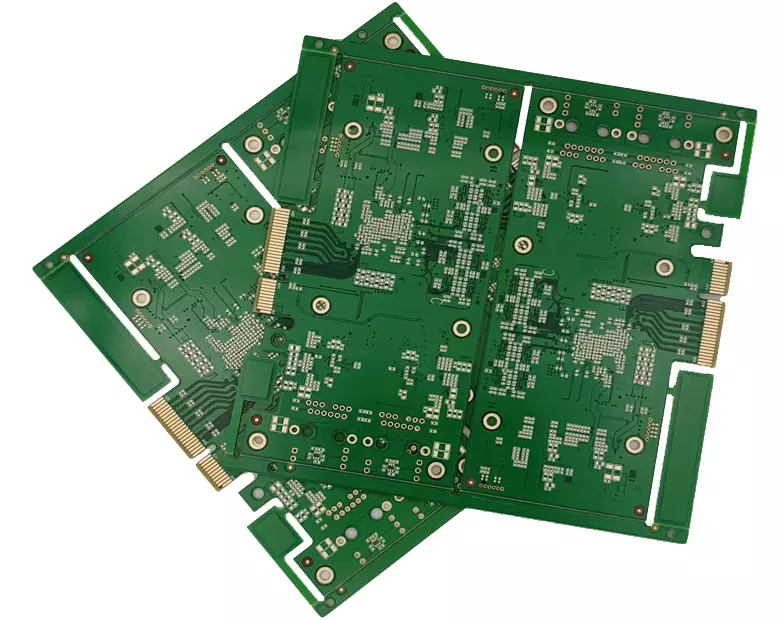
HDI PCB, serving as the core carriers for high-end electronic devices, meets the demands for miniaturisation and high performance through their high-density interconnect characteristics. However, complex processes such as laser drilling and multi-layer buried/blind vias also drive up manufacturing costs. Many enterprises in HDI PCB applications often fall into the misconception of ‘achieving performance targets regardless of cost’, overlooking the decisive influence of the design phase on expenditure. Without compromising core performance, optimising three key design techniques – tier planning, hole configuration design, and material adaptation – can achieve cost reductions of 10%-30%. This simultaneously ensures mass production stability, establishing a cost-performance advantage for end products.
Core Principles of Design Cost Control
The essence of reducing HDI PCB costs lies not in mere specification cuts, but in achieving a triangular equilibrium through design optimisation: meeting performance requirements, optimising costs, and ensuring mass production feasibility. All design techniques must be implemented through deep collaboration with manufacturers—pre-confirming process windows, identifying cost-sensitive points, and avoiding rework or scrap costs caused by design-manufacturing disconnects.
Concurrently, consideration must extend to the product’s full lifecycle cost rather than focusing solely on the manufacturing cost per PCB. For instance, while simplifying the design may slightly increase design man-hours, it can significantly enhance mass production yield and reduce subsequent maintenance costs, resulting in superior overall cost-effectiveness. With the widespread adoption of HDI PCB technology and the maturation of domestic manufacturing processes, cost control opportunities at the design stage will expand further. Through precise design optimisation, HDI PCBs can achieve dual adaptability for both high-end applications and cost-performance scenarios, thereby enhancing the market competitiveness of end products.
Methods for Reducing HDI PCB Costs:
1.Combining on-demand layer reduction with buried/blind vias to avoid premium costs associated with higher-layer processes
HDI PCB costs correlate positively with layer count. Each additional layer significantly increases complexity in laser micro-via processing, layer-to-layer alignment, and electroplating, driving cost increases of 20%-25%. Many designs unnecessarily pursue high-layer HDI for redundancy, when most scenarios can achieve performance requirements while eliminating premium costs through a judicious combination of layer reduction and buried/blind vias.
The core principle is to match the layer count to signal requirements rather than indiscriminately pursuing high specifications. For consumer electronics (such as smartphone mid-frame modules) and standard industrial control equipment, where pin pitch exceeds 0.5mm and high-frequency signals constitute less than 30% of the total, 1-2 layer HDI can fully replace 3-layer or higher solutions. First-level buried vias facilitate inner-layer signal interconnections, while second-level blind vias link top layers to inner layers. Combined with localised laser microvias to optimise fan-out, this approach meets routing density requirements while eliminating equipment depreciation and labour costs associated with higher-order processes. Practical data from a consumer electronics manufacturer indicates that optimising the original tier-3 HDI solution to a tier-2 + localised buried/blind via combination reduced single-PCB costs by 22% and increased mass production yield from 92% to 96%.
Pay particular attention to the rationality of interlayer interconnections to avoid redundant buried/blind via designs. Certain designs feature redundant ‘full-level blind vias on every layer’ operations. Consolidating signal layers of similar types and optimising pin fan-out paths can reduce the number of buried/blind vias. For instance, integrating power signals with low-frequency control signals onto the same inner layer and sharing buried vias for interconnection can reduce blind via usage by 15%-20% per PCB, further compressing manufacturing costs. Concurrently, manufacturers’ capabilities must be confirmed in advance to ensure downgrading schemes align with mass production process windows, thereby avoiding rework costs stemming from design-manufacturing mismatches.
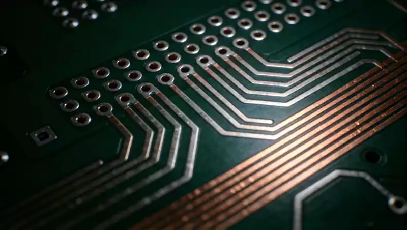
2.Hole Pattern Optimisation + Routing Streamlining to Reduce Microvia Processing Costs
Laser microvia formation constitutes one of the core processes in HDI PCB manufacturing, accounting for over 35% of total production costs. Hole diameter, microvia count, and hole distribution directly impact processing efficiency and consumable wastage. By precisely optimising hole parameters and routing rules, microvia processing costs can be substantially reduced without compromising signal integrity.
Prioritise enlarging microvia apertures for non-critical signals to reduce laser processing time. Conventional HDI PCB microvia apertures range from 0.075–0.1mm; each 0.02mm reduction in aperture diameter decreases processing speed by 30% and increases material wastage by 18%. For non-critical links such as low-frequency control signals and auxiliary power signals, microvia apertures can be optimised to 0.12–0.15mm. These can be processed using conventional laser equipment without requiring high-precision slow-speed modes, reducing microvia processing time per PCB by 40%. Simultaneously, controlling the aspect ratio of microvias within 1:1.5 reduces plating complexity, enhances conductivity stability, and minimises copper plating material consumption, further compressing costs.
Routing optimisation reduces microvia count by eliminating redundant apertures. BGA fan-out paths are refined using Via-in-Pad technology to replace conventional peripheral vias, decreasing required microvia density. In high-density pin areas, rational routing channel planning avoids unnecessary apertures caused by detours. In the design of an automotive ADAS module, optimising BGA fan-out and routing layout reduced microvia density from 80 to 55 per square centimetre, lowering per-PCB costs by 15%. Furthermore, standardising microvia specifications eliminates the need for multiple aperture designs, reducing laser equipment parameter switching frequency. This enhances batch processing efficiency and lowers equipment debugging costs.
3.Material Adaptation + Process Simplification: Eliminating Redundant Costs
HDI PCB materials and surface treatment processes often suffer from cost wastage due to ‘over-specification’. By precisely matching material grades and process types to product application scenarios, reliability is ensured while significantly reducing material costs.
Material selection must dispel the misconception that ‘high-end equals optimal’; instead, adapt laminate and copper foil specifications to specific scenarios. High-frequency signal applications (e.g., millimetre-wave radar, 5G modules) require low-dielectric loss laminates (e.g., Rogers 4350B). However, conventional FR-4 laminates (e.g., S1000-2) suffice for low-frequency consumer electronics and standard industrial equipment, reducing material costs by 40%-50%. Copper foil thickness may likewise be optimised as required. Reducing signal layer copper foil from 1oz to 0.5oz lowers material costs by 12% without compromising low-frequency signal transmission; power planes may retain 1oz copper foil to ensure current-carrying capacity. In the optimisation of an automotive central control module design, replacing the original high-frequency substrate with cost-effective FR-4 material, combined with copper thickness adjustments, reduced the material cost per PCB by 38%. Performance fully met automotive standards following high-low temperature cycling tests.
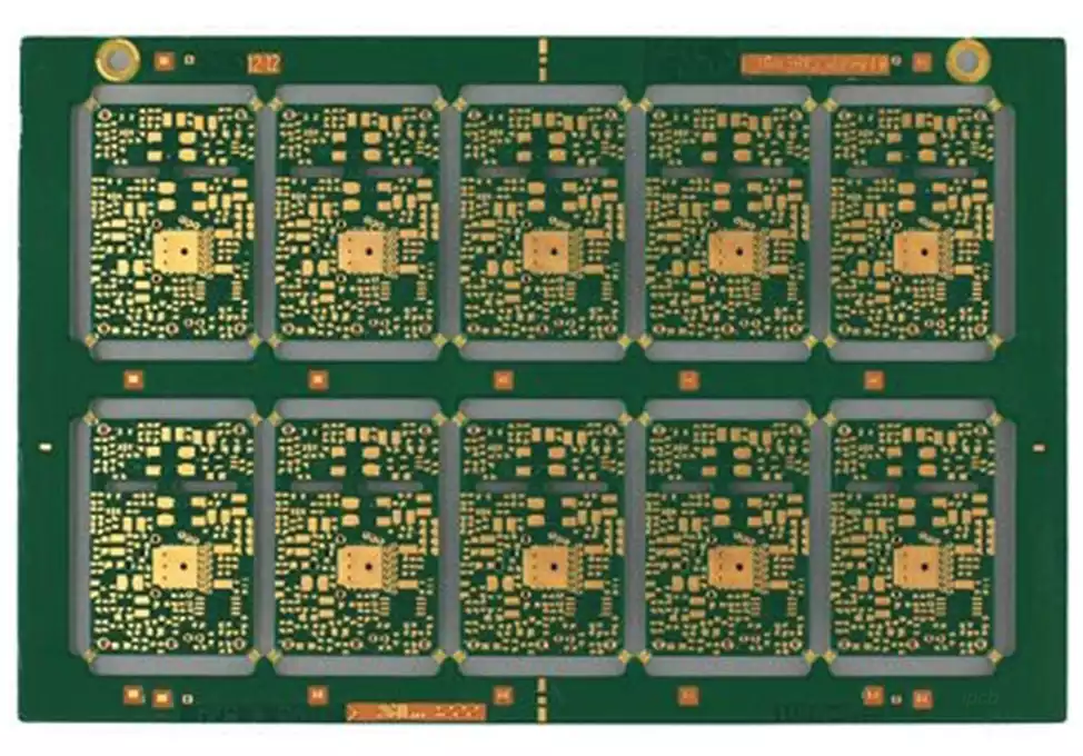
Simplify surface finishing processes to eliminate redundant protection. Significant cost variations exist between different surface treatments. Under standard conditions, Hot Air Solder Leveling (HASL) offers the lowest cost, while Electroless Nickel Immersion Gold (ENIG) costs approximately 2.5 times more. Electrolytic silver and tin plating fall between these two in cost. For non-high-frequency, non-precision soldering applications, HASL should be prioritised. Where soldering reliability requires enhancement, electroless silver plating may replace ENIG, reducing costs by over 40%. Simultaneously, eliminating unnecessary localised gold plating—reserving it solely for critical soldering areas while applying conventional treatments elsewhere—further compresses process costs. Furthermore, standardising PCB dimensions and panelisation schemes to enhance material utilisation and minimise scrap waste serves as a crucial supplementary measure for reducing material costs.
In summary, employing three key design techniques, collaborating with manufacturers and considering the full lifecycle cost can effectively reduce HDI PCB costs.