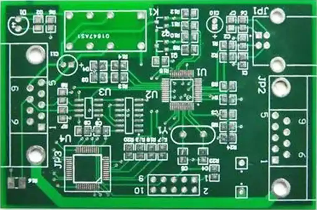
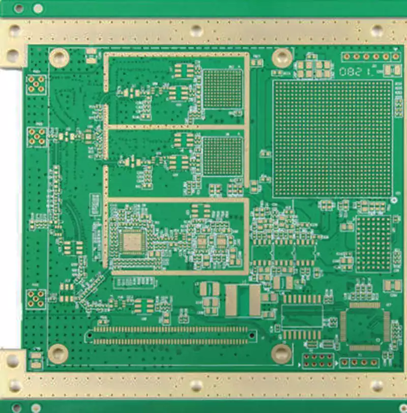
Impedance Boards (commonly referred to as impedance boards) are specialized circuit boards in PCB manufacturing that require precise design, calculation, and strict production control of signal trace characteristic impedance. Their core value lies in ensuring signal transmission stability. Unlike conventional PCBs that only ensure electrical connectivity, impedance boards impose stringent requirements on impedance deviation throughout the manufacturing process.
Production tolerance for impedance Boards refers to the allowable deviation between the actual measured impedance value and the designed target impedance. It also encompasses tolerance control of related parameters such as trace width and dielectric thickness. The level of tolerance control directly determines the signal integrity of the final product. It not only reflects a PCB manufacturer’s process capability, but is also a critical factor in ensuring product qualification and controlling manufacturing costs.
Specifically, impedance board production tolerance is defined as the maximum allowable deviation between the actual impedance value and the target design impedance during manufacturing, while also covering tolerance control of key parameters affecting impedance stability (such as trace width, dielectric thickness, copper thickness, etc.). Among these, the setting of impedance tolerance ranges must be adjusted according to different end-use application scenarios, which represents the most critical control focus within the industry.
Challenges in Impedance Tolerance Control
In actual production, impedance tolerance control faces numerous challenges, which are common pain points across most PCB manufacturers.
First, there is strong parameter interdependence, where deviation in a single process step can trigger a chain reaction. For example, a trace width deviation of 0.03 mm or a dielectric thickness deviation of 0.02 mm may cause the impedance to exceed the allowable range. In production, these parameters often influence each other, making isolated control difficult.
Second, raw material variation is difficult to control. Variations in dielectric constant across different laminate batches, as well as copper foil thickness deviations, can undermine impedance consistency at the source. This issue is especially critical for low-loss, high-frequency materials, where even slight material fluctuations can significantly affect impedance stability.
Third, process control blind spots exist. Some manufacturers rely excessively on manual operations and lack real-time monitoring of critical processes such as etching and lamination. As a result, impedance tolerance deviations may occur during mass production without timely detection or correction.
Fourth, impedance testing is often delayed. Many manufacturers only perform impedance testing at the finished-product stage. Once deviations are discovered, substantial raw material waste has already occurred, leading to increased production costs.
Key Factors Affecting Impedance Board Production Tolerance
The impedance value of an impedance Board is primarily determined by five core factors: transmission line structure, substrate dielectric constant (εr), dielectric thickness (h), trace width (w), and copper thickness (t). Impedance calculation follows IPC-2141 standard formulas. Variations in these five factors are the root causes of impedance tolerance deviation. Only by accurately analyzing the influence mechanism of each factor can targeted control strategies be established.
Dielectric Thickness and Dielectric Constant
Dielectric thickness and dielectric constant are the “core carrier factors” affecting impedance tolerance. As the foundation of impedance transmission, uniformity of dielectric thickness directly determines impedance stability. Impedance is positively correlated with dielectric thickness—the thicker the dielectric layer, the higher the impedance, and vice versa.
For example, in a 12-layer impedance board used for 5G base stations, if the designed dielectric thickness is 0.1 mm, a thickness deviation of 0.02 mm combined with a dielectric constant fluctuation of 0.2 may result in an impedance deviation exceeding 8%, far beyond typical tolerance limits. Dielectric constant stability is equally critical. At different frequency ranges, dielectric constant variation directly alters impedance calculation results. In high-frequency applications, low-loss materials with dielectric constant fluctuation ≤ ±0.2 are required; otherwise, impedance values will continuously fluctuate and fail to meet tolerance requirements.
In addition, lamination process precision directly affects dielectric thickness uniformity. Deviations in lamination temperature, pressure, or time can all cause non-uniform dielectric thickness, leading to impedance tolerance violations.
Trace Width and Copper Thickness
Trace width and copper thickness are the “key structural factors” influencing impedance tolerance. Trace width is negatively correlated with impedance—the wider the trace, the lower the impedance. Trace width deviation is one of the most common causes of impedance out-of-tolerance conditions.
In the industry, impedance trace width tolerance is typically controlled within ±5% to ±10%, which is significantly stricter than that for standard signal traces. For example, if the designed impedance trace width is 0.20 mm with a ±10% tolerance, the etched trace width must be controlled within 0.20–0.22 mm to prevent micro-etching during brown oxidation or rework processes from degrading impedance stability.
Copper thickness is also negatively correlated with impedance. Thicker copper reduces impedance and increases signal loss if not properly controlled. Inner-layer copper thickness is typically managed at 1 oz or 2 oz with tight control, while plated copper thickness deviation should be ≤ ±8%. Real-time monitoring is required to ensure consistency and prevent impedance deviation caused by copper thickness fluctuation.
Secondary Influencing Factors
In addition to the five core factors, production environment and process details indirectly affect impedance tolerance. Workshop temperature and humidity fluctuations (recommended control: 23 °C ± 2 °C, 50% ± 5% RH) can cause substrate expansion or contraction, affecting trace width and dielectric thickness. Etching solution concentration and etching speed variations can lead to uneven trace profiles, such as necking or rough edges, which compromise impedance consistency.
Solder mask thickness also plays a significant role. Solder mask thickness is negatively correlated with impedance; typically, solder mask application reduces single-ended impedance by 2–4 Ω and differential impedance by 3–8 Ω. Non-uniform solder mask thickness may therefore cause impedance to exceed allowable tolerance. Additionally, phototool cleanliness and exposure accuracy indirectly affect trace width precision and thus impedance tolerance.
Impedance Board Production Tolerance Control Strategies
Raw materials represent the first line of defense in impedance tolerance control and are often the most overlooked factor. Only by controlling raw material quality at the source can downstream process pressure be reduced and impedance consistency ensured.
Laminate Selection and Control
Material selection must be tailored to end-use scenarios. For standard high-speed applications, conventional laminates such as Shengyi S1130 may be used, with dielectric constant controlled at 4.3 ± 0.2. For mid- to high-end high-frequency applications, low-loss materials such as Rogers RO4350B or Panasonic high-frequency laminates should be selected, with dielectric constant fluctuation ≤ ±0.1 and dissipation factor ≤ 0.0037 at 10 GHz.
A full incoming inspection mechanism should be established. Before warehousing, each laminate batch must be tested for dielectric constant, thickness uniformity, and thermal resistance. Sampling inspection should not be less than 5%, and nonconforming materials must be rejected. After warehousing, materials should be stored by batch with clear identification to prevent batch mixing. Self-pressed core boards must be strictly prohibited for impedance board production, as lamination thickness cannot be accurately controlled.
Copper Foil and Auxiliary Materials
High-quality copper foil with thickness deviation ≤ ±8% should be selected, preferably from reputable suppliers. Incoming inspection should include copper thickness and adhesion testing to avoid oxidation or non-uniform thickness. Auxiliary materials such as prepregs and solder mask must be compatible with the laminate system. Prepreg resin content and thickness must strictly follow MI requirements, and thickness uniformity should be verified before lamination. Solder mask materials with stable dielectric properties should be selected to ensure uniform coating and minimal impedance impact.
Core Process Control: Exposure, Etching, and Lamination
The main sources of impedance tolerance variation lie in the manufacturing process, particularly exposure, etching, and lamination. A control model of “first article verification + real-time monitoring + closed-loop parameter adjustment” should be established.
Exposure Control focuses on trace width accuracy. Phototools must be thoroughly inspected before exposure to ensure compliance with MI requirements. First article boards must be produced and inspected using high-magnification measurement equipment. Only after QA approval can mass production proceed. During production, strict cleanliness standards must be enforced to prevent contamination-induced line width deviation.
Etching Control is the most critical stage for impedance tolerance. Etching parameters must be adjusted based on first article results to ensure uniform etching. After etching, impedance values should be controlled near the upper tolerance limit to reserve margin for solder mask impact. Increased inspection frequency is required during mass production, with immediate corrective actions if abnormalities are detected. Rework should be strictly limited to a single occurrence to avoid excessive line narrowing and copper loss.
Lamination Control focuses on dielectric thickness uniformity and layer alignment. First article lamination must include full thickness measurement and microsection analysis. During mass production, lamination parameters should be tightly controlled, and layer alignment accuracy maintained within ±0.01 mm to prevent transmission line deformation.
Fine Control of Plating and Solder Mask Processes
During pattern plating, fixture methods and plating parameters must ensure uniform copper thickness. First article verification is mandatory for new part numbers. In the solder mask process, standard parameters apply for normal products, while impedance-adjustment strategies through solder mask thickness control may be used for borderline cases, validated through first article testing.
Future Trends in Impedance Tolerance Control
With the rapid development of 5G millimeter-wave technology, high-speed servers, automotive electronics, and medical devices, impedance tolerance control is evolving toward higher precision, intelligence, and full-process integration.
Tolerance requirements in high-end applications will continue to tighten, with ±3% or even ±2% becoming mainstream. Intelligent manufacturing systems using AI-based real-time monitoring will gradually replace manual control, enabling proactive prevention rather than reactive correction. Moreover, full-process collaboration between design, manufacturing, and testing will become standard, forming closed-loop optimization systems.
For PCB manufacturers, impedance tolerance control is both a technical challenge and a strategic opportunity. Only through comprehensive, fine-grained control across the entire process—supported by continuous technological and equipment upgrades—can manufacturers deliver high-end Impedance Boards, strengthen brand reputation, and secure competitive advantage in demanding markets.