In the era where electronic devices are constantly evolving towards higher performance and greater integration, the heat dissipation issue of PCBs has become increasingly critical. Copper, with its outstanding thermal conductivity, has become the core carrier for PCB heat dissipation design. Compared to FR-4 substrate material, copper has a significantly superior thermal conductivity. Rational utilization of copper foil to construct a heat dissipation network can effectively solve heat dissipation challenges. For 4 layer pcbs, efficient heat dissipation solutions can be developed by optimizing the stack-up structure, designing heat dissipation vias, reasonably arranging components, and utilizing external heat dissipation aids and simulation optimization, thereby ensuring the stable operation of electronic devices.
Copper is the core carrier for PCB heat dissipation design, and its excellent thermal conductivity makes it an ideal heat dissipation material. Compared to the thermal conductivity of 0.3 W/mK for FR-4 substrate material, copper’s thermal conductivity is as high as 380 W/mK, which is thousands of times that of the substrate material. Therefore, by configuring a sufficiently large copper area for the heat source and opening up “thermal channels” to other layers, an efficient three-dimensional heat dissipation network can be formed. Increasing the copper foil area can effectively reduce thermal resistance, thereby significantly improving heat dissipation efficiency. When the copper foil area increases, heat can be conducted from the heat-generating components to the surrounding environment through a wider range of paths, thus avoiding the occurrence of local overheating.
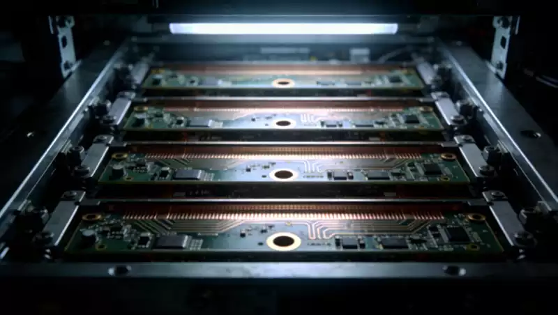
Stack-up Structure Optimization and Inner-layer Copper Foil Application for 4 layer pcbs
Multilayer PCBs offer far superior heat dissipation performance compared to single-layer and double-layer PCBs because they can utilize inner-layer copper foil to form a “three-dimensional heat dissipation network” that effectively conducts heat away. For 4 layer pcbs, it is recommended to adopt a stack-up structure of signal layer-ground plane-power plane-signal layer. Among them, the ground plane and power plane should feature a continuous copper foil design (with a thickness of 2 oz), and the spacing between divided areas on the power plane should be less than or equal to 5 mm to ensure effective heat conduction and diffusion.
Optimizing Stack-up Structure to Maximize Heat Dissipation Efficiency
Optimizing the stack-up structure of a PCB is the first step in solving heat dissipation problems. For 4 layer pcbs, the internal layers can be fully utilized to construct efficient heat dissipation channels.
Large-area Ground Plane and Power Plane: Design the ground or power plane as a continuous large-area copper foil to leverage copper’s excellent thermal conductivity and provide a fast heat conduction path. For example, in server motherboard design, the large-area copper foil ground plane within the multilayer board can uniformly disperse the heat generated by various chips and conduct it to the chassis enclosure or heat sinks. This design not only aids in heat dissipation but also improves electromagnetic compatibility (EMI) and signal integrity.
Application of Thick Copper Foil: Increasing the copper layer thickness, especially on the inner layers, can significantly enhance thermal conductivity. Tests conducted by 4 layer pcb manufacturers show that optimized thick copper foil heat dissipation channels can improve heat conduction efficiency by 60% and reduce chip junction temperatures by 15-20°C. Although processing costs increase by 20%, this eliminates the need for more expensive heat sinks, demonstrating economic benefits in high-power products.
Multilayer Board Integration: In multilayer PCBs, widening the inner-layer copper foil can achieve three-dimensional heat dissipation. Directly widening the copper foil around high-power components (such as processors or power ICs) can effectively reduce temperatures. For example, widening the copper foil around the CPU on a server motherboard can lower temperatures by 10-15%, thereby enhancing stability.
Heat Dissipation Vias and Thermal Channel Design
In 4 layer pcb design, heat dissipation vias are crucial for connecting different copper layers and achieving vertical heat conduction.
Dense Array of Vias: By using a dense array of vias, heat can be quickly directed from heat-generating components to the inner-layer copper foil. These vias should be placed beneath thermal-sensitive components and high-power devices.
Via Size and Quantity: The diameter and quantity of vias have a significant impact on heat dissipation performance. Practice shows that increasing the number of vias can effectively reduce thermal resistance. It is generally recommended to use vias with a diameter of 20 mil (approximately 0.5 mm) directly beneath heat dissipation pads.
Filling and Blocking Vias: To prevent solder from being sucked into vias and affecting heat conduction efficiency, vias can be filled or blocked, especially in cases where there is solder beneath exposed pads or fins. It is recommended to use vias with a size of less than 0.3 mm in such scenarios. Conductive-filled vias not only enhance conductivity but also improve heat transfer performance.
Stitching Vias: Stitching vias can be used to connect larger copper areas on different layers, forming a robust vertical connection that aids in heat transfer and improves signal integrity as well as EMI/EMC performance.
Component Layout and Hotspot Management
Reasonable component layout is the foundation of heat dissipation design.
Dispersing Heat Sources: Disperse heat-generating components, such as power amplifiers, CPUs, and GPUs, across the PCB to avoid excessive heat concentration and the formation of “hot islands.”
Optimized Placement: Place components with the highest power consumption and heat generation near the best heat dissipation locations, avoiding placement in the corners and edges of the printed circuit board unless there are heat dissipation devices nearby. High-power devices should be placed as close to the center of the printed board as possible to facilitate heat dissipation in all directions along the surface.
Avoiding Hotspot Concentration: Distribute power as evenly as possible across the PCB to maintain uniform and consistent surface temperature performance, thereby avoiding hotspots that can affect the normal operation of the entire circuit.
External Heat Dissipation Aids and Simulation Optimization
When the PCB’s own heat dissipation means are insufficient to meet requirements, external heat dissipation devices are necessary.
Heat Sinks and Heat Pipes: For a few components with high heat generation, heat sinks or heat pipes can be added. If temperatures still cannot be lowered, heat sinks with fans can be used to enhance heat dissipation effects.
Thermal Simulation Tools: During the PCB design phase, professional thermal simulation software (such as Flotherm and Icepak) can be used to simulate heat dissipation performance under different operating conditions. Based on the simulation results, potential heat dissipation problems can be identified in advance, and design schemes can be adjusted, thereby significantly improving design success rates and efficiency.
The heat dissipation design of 4 layer pcbs is a systematic project involving stack-up structure optimization, heat dissipation via design, component layout, external heat dissipation aids, and simulation optimization. By rationally applying these design techniques and fully leveraging the thermal conductivity advantages of copper foil, heat dissipation efficiency of PCBs can be effectively improved, local overheating can be avoided, and electronic devices can be ensured to operate stably and reliably under various operating conditions. In actual design processes, designers need to flexibly adjust and optimize heat dissipation schemes according to specific product requirements and application scenarios to achieve the best heat dissipation effects.