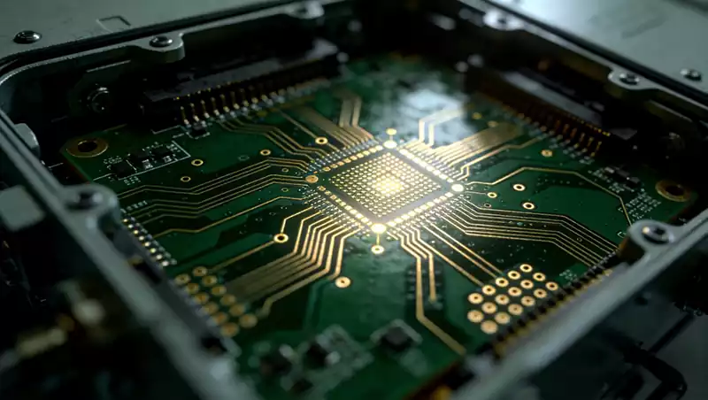
In the current era where 5G communication technology is reshaping the global information landscape with lightning speed, 5G base stations, serving as the “nerve endings” of network coverage, directly determine user experience and communication quality through their performance stability. Hidden within these base stations, high speed high frequency boards function like precise “nerve pathways.” With millimeter-level precision, nanosecond-level response times, and exceptional reliability in extreme environments, they form the cornerstone supporting 5G networks’ high data rates, low latency, and massive connectivity.
Unlike conventional PCBs in the consumer electronics sector, high-speed high frequency boards in 5G base stations face four core challenges: high frequency losses, signal interference, high-temperature aging, and precision control. The design and manufacturing logic of conventional PCBs are entirely inadequate here—even a 0.01mm deviation in circuit lines or a 0.1 variation in dielectric constant can lead to over 50% signal attenuation and base station failure. This article draws on frontline experience in the PCB manufacturing industry to dissect the core design considerations, manufacturing challenges, and optimization solutions for high-speed high-frequency circuit boards in 5G base stations. Combining professionalism with accessibility, it offers unique industry insights and practical references for engineers and procurement professionals, highlighting the technical responsibility of the PCB manufacturing sector in the 5G communication landscape.
The Critical Role of High Speed High Frequency Boards in 5G Base Stations
The normal operation of a 5G base station relies on the coordinated work of the Radio Frequency Unit (RRU), Baseband Unit (BBU), and Antenna Array Unit (AAU). The core connections and signal transmission among these three units are entirely facilitated by high-speed high frequency boards, which act as the “neural network” of the base station. These boards are responsible for converting baseband signals into high-frequency radio frequency signals and demodulating received high-frequency signals back into baseband signals, while also supporting high-speed data interactions. Their performance directly determines the core experience of 5G networks.
Compared to ordinary PCBs, the irreplaceability of high-speed high frequency boards in 5G base stations is concentrated in three core dimensions, which are also the key technical challenges for the PCB manufacturing industry:
High-Frequency Adaptability: They must stably carry high-frequency signals in both the Sub-6GHz (mainstream frequency band) and millimeter-wave (future expansion band) ranges, with dielectric and conductor losses kept at extremely low levels to prevent severe signal attenuation during transmission. Ordinary PCBs lose over 60% of signals every 10cm at 10GHz, making them utterly inadequate for base station requirements.
High-Speed Transmission: They need to be compatible with high-speed links such as CPRI interfaces and Ethernet, supporting data transmission rates exceeding 100Gbps without signal delay, jitter, or errors. This places extreme demands on impedance control and wiring precision.
High Reliability: 5G base stations are mostly deployed outdoors, enduring extreme temperature variations from -55°C to 125°C, rain, wind erosion, and vibration impacts. The circuit boards must exhibit strong resistance to aging, corrosion, and thermal stress, meeting the highest reliability standard of IPC-6012 Class 3/A.
For the PCB manufacturing industry, the research and production of high-speed high-frequency circuit boards for 5G base stations represent not only an opportunity for technological upgrades but also a key to seizing industry leadership. These boards break through the technical barriers of conventional PCBs, integrating core technologies such as high-frequency materials, precision manufacturing, and signal simulation. Their manufacturing standards directly reflect the core competitiveness of a PCB enterprise and serve as a crucial support for the implementation of 5G communication technology.
Core Technical Requirements for High-Speed High Frequency Boards in 5G Base Stations
The requirements for high-speed high frequency boards in 5G base stations are far more stringent than those for ordinary electronic devices, focusing on four dimensions: materials, precision, reliability, and heat dissipation, with each requirement precise to the micrometer level. These demands test both the design capabilities and manufacturing process refinement of PCB enterprises, serving as the core criteria distinguishing conventional PCBs from 5G-specific PCBs and guiding the upgrading direction of the PCB manufacturing industry.
Substrate Selection
The substrate is the “foundation” of high-speed high frequency boards, with its dielectric constant (εr) and dielectric loss tangent (tanδ) directly determining the quality of high-frequency signal transmission, forming the core basis for substrate selection. Substrates for high-speed high-frequency circuit boards in 5G base stations must meet four requirements: low dielectric constant, low loss, high stability, and high-temperature resistance, with different frequency bands requiring tailored substrate selections to balance performance and cost.
Specifically, the millimeter-wave frequency band (24-300GHz) imposes the most stringent requirements on substrates, necessitating the use of special substrates with a low and stable dielectric constant (εr = 2.0-3.0) and extremely low dielectric loss (tanδ ≤ 0.0025). Preferred materials include PTFE (polytetrafluoroethylene) and Rogers RO4835 (εr = 3.48, tanδ = 0.0037), which exhibit minimal dielectric constant variations with frequency and temperature, effectively reducing dielectric losses in high-frequency signals and ensuring transmission stability. For the Sub-6GHz frequency band, modified FR-4 substrates (e.g., FR-408) can be used, with a dielectric constant around 3.8 and a dielectric loss tanδ ≤ 0.008, meeting high-frequency transmission needs while controlling manufacturing costs, and complying with the specialized technical specifications for high-frequency substrates in IPC-4101.
Additionally, the heat resistance and dimensional stability of substrates are crucial. The power amplifier area in the RRU of a 5G base station can reach temperatures above 100°C, requiring substrates with a glass transition temperature (Tg) ≥ 180°C to prevent board deformation or delamination under high temperatures. Meanwhile, the coefficient of thermal expansion (CTE) of the substrate must match that of copper foil to reduce line breakage and via failure caused by thermal stress, extending the board’s service life.
Precision Control
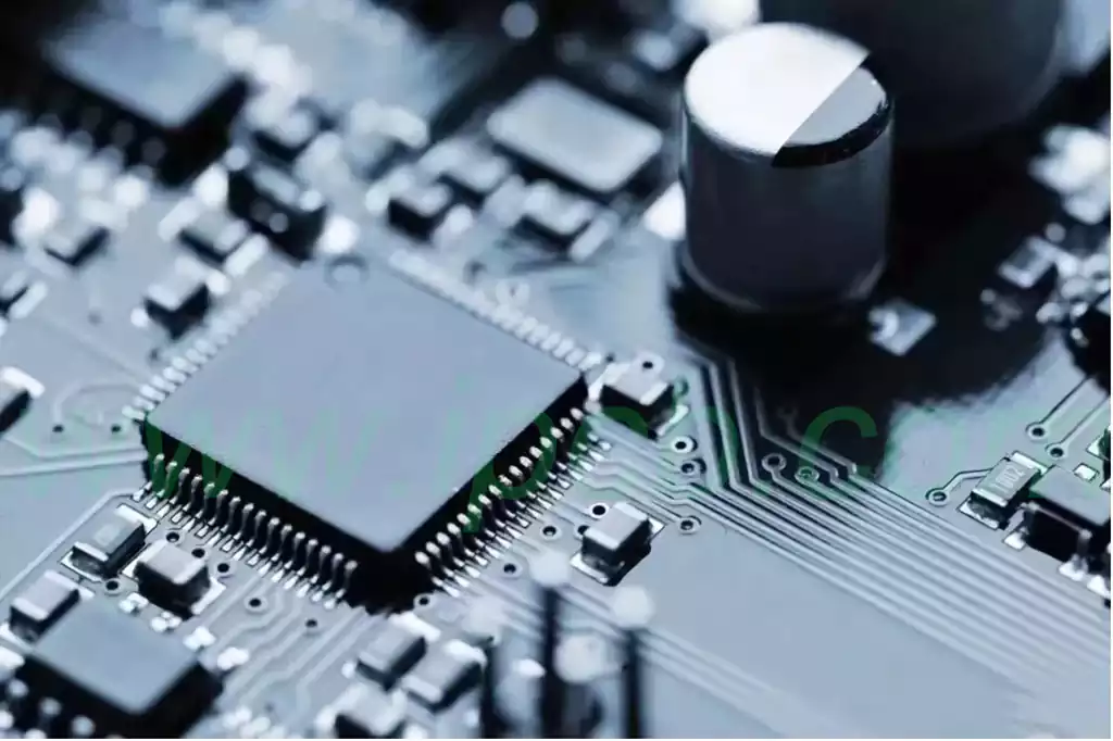
High-speed high-frequency signals are highly sensitive to circuit board precision, with minor deviations in line width, line spacing, and via dimensions causing impedance mutations, signal reflections, and crosstalk, affecting transmission quality. Precision control for high speed high frequency boards in 5G base stations must reach the micrometer level, focusing on three core aspects: lines, vias, and impedance, reflecting the precision manufacturing capabilities of the PCB manufacturing industry.
Line Precision: The width deviation of high-frequency radio frequency lines must be controlled within ±0.005mm, and the line spacing deviation ≤ ±0.01mm to avoid impedance shifts due to overly wide or narrow lines. High-speed differential lines (e.g., for CPRI interfaces) must strictly adhere to the “equal length and equal spacing” principle, with length errors < 0.5mm and spacing deviations < 0.02mm, reducing signal errors caused by timing differences. Wiring should use arc transitions (radius ≥ 3 times the line width) to prevent signal scattering from right or sharp angles. Copper foil selection is also critical, requiring Very Low Profile (VLP) copper foil with a surface roughness (Ra) ≤ 0.3μm to reduce skin effect losses in high-frequency signals—at 10GHz, current concentrates within 5μm of the copper foil surface, and rough surfaces exacerbate signal scattering, while VLP copper foil can reduce transmission losses for 28GHz signals by 15%-20%.
Via Design: Vias should follow the principles of “miniaturization and minimalism,” with diameters reduced from 0.3mm in ordinary PCBs to 0.15-0.2mm, and copper plating thickness on via walls ≥ 20μm to reduce signal reflections and losses caused by vias. Additionally, the number of vias should be minimized to avoid disrupting line continuity and affecting signal transmission.
Impedance Control: High-frequency radio frequency lines must maintain an impedance of 50Ω, while high-speed differential lines must maintain 100Ω, with impedance tolerances ≤ ±3% (≤ ±2% for millimeter-wave frequency bands). Precise calculations of line width, line spacing, and substrate thickness, combined with impedance simulation technology, are required to ensure impedance consistency.
Reliability and Heat Dissipation
5G base stations are mostly deployed outdoors on towers or rooftops, facing complex environments with extreme temperatures, rain, wind, and vibrations. Meanwhile, power amplifiers, chips, and other components inside the base station generate significant heat. Therefore, high speed high frequency boards must exhibit strong reliability and heat dissipation capabilities, which are crucial for ensuring the long-term stable operation of base stations.
Reliability: Circuit boards must pass rigorous environmental tests, including temperature cycling tests (-55°C to 125°C, over 1000 cycles), humidity tests (95% relative humidity, 85°C, 1000 hours), and vibration tests (10-2000Hz, 10G acceleration). After testing, there should be no delamination, line breakage, or solder joint detachment, with insertion loss changes ≤ 0.5dB. Surface treatments should use lead-free tin plating or nickel-gold plating to enhance corrosion and oxidation resistance, preventing line oxidation failures in outdoor environments.
Heat Dissipation: Efficient heat dissipation systems must be integrated through PCB design and manufacturing processes. High-heat areas (e.g., beneath power amplifier chips) should use thick copper foil (2oz or 70μm or more) to increase heat dissipation area and reduce conductor losses. Thermal via arrays (0.3mm diameter, 1mm spacing) should be arranged to conduct surface heat to inner-layer copper foil for rapid heat diffusion. Additionally, metal substrates or embedded copper blocks can be used as auxiliary heat dissipation structures. For high-power base stations, heat sinks and thermal conductive adhesives can be combined to keep device junction temperatures below 85°C, preventing device aging and circuit board failures caused by high temperatures.
Overcoming Core Design and Manufacturing Challenges
Despite the stringent technical requirements for high speed high frequency boards in 5G base stations, the PCB manufacturing industry has developed mature practical solutions through technological research and process optimization, effectively addressing the three core challenges of “high-frequency losses, precision control, and reliability” while balancing performance and cost to support the large-scale deployment of 5G base stations. Based on frontline experience, this section dissects the techniques for overcoming these core challenges to provide industry references.
Excessive High-Frequency Signal Losses
Solution: In addition to using low dielectric constant, low-loss substrates and VLP copper foil, signal losses can be further reduced by optimizing wiring design to shorten high-frequency line lengths and minimize signal transmission paths. Shielding grounding designs can be employed, with ground isolation strips placed between high-frequency lines and sensitive lines to reduce signal crosstalk. High-frequency signal simulation technology can be used during the initial design phase to simulate signal transmission effects and optimize line layouts in advance to avoid loss risks. Practical tests show that with these solutions, the transmission loss per centimeter for 28GHz millimeter-wave signals can be reduced to below 0.3dB, meeting the requirements for long-distance transmission in base stations.
High Difficulty in Micrometer-Level Precision Control
Solution: Laser Direct Imaging (LDI) technology can be introduced to replace traditional exposure technology, controlling line precision within ±0.005mm and improving line uniformity and consistency. High-precision lamination processes, combined with optical positioning systems, can ensure interlayer alignment deviations ≤ 10μm (about 1/5 the diameter of a human hair) in multilayer boards, avoiding impedance mutations caused by interlayer deviations. The etching process can adopt an “acid etching + additive” scheme to control undercutting within 2μm, ensuring vertical and steep line edges to reduce signal scattering.
Insufficient Reliability in Outdoor Environments
Solution: Optimize substrate and auxiliary material selections by using high-temperature-resistant, aging-resistant substrates and adhesives to enhance the circuit board’s resistance to thermal stress. Adopt a “full-board solder mask coverage” process to strengthen the board’s corrosion and moisture resistance, preventing erosion from outdoor rain and wind. Use via plugging and sealing processes in via designs to prevent water vapor from entering vias and causing short circuits. Meanwhile, strengthen quality control during manufacturing by strictly testing raw materials such as substrates, copper foil, and plating solutions, and precisely controlling processes like lamination, etching, and soldering to ensure every circuit board meets reliability standards.
Future Trends for High Speed High Frequency Boards in 5G Base Stations
Deeper Extension into Millimeter-Wave Frequencies
As millimeter-wave frequency bands become commercially viable, the high-frequency performance requirements for circuit boards will further increase, with dielectric constants needing to drop to around 2.0, dielectric loss tangents tanδ ≤ 0.002, and line precision controlled within ±0.003mm. This will drive PCB substrates to upgrade to higher-quality special materials, while promoting further optimization of laser drilling, precision etching, and other processes to break through technical barriers in millimeter-wave frequency bands.
Integration of Integration and Miniaturization
5G base stations are evolving toward miniaturization and integration, with AAU (Antenna Array Unit) and RRU (Radio Frequency Unit) integration requiring high-speed high frequency boards to achieve High-Density Interconnect (HDI), integrating more lines and components within limited space. This will drive the deep integration of HDI technology with high-speed high-frequency PCBs, using micro-blind vias and buried vias to reduce circuit board size and enhance integration while maintaining high-speed transmission and high-frequency performance.
Parallel Development of Intelligence and Green Manufacturing
In the future, the PCB manufacturing industry will introduce intelligent technologies such as AI and big data to enable intelligent design, simulation, and manufacturing of high speed high frequency boards, improving design efficiency and reducing trial-and-error costs. Meanwhile, green manufacturing will become an industry consensus, with research into environmentally friendly low-loss substrates and promotion of lead-free and halogen-free manufacturing processes to reduce pollutant emissions and achieve dual goals of technological upgrading and environmental protection.
High speed high frequency boards for 5G base stations are the core carriers for implementing 5G communication technology and a key direction for technological upgrading in the PCB manufacturing industry. Their design and manufacturing integrate multiple core technologies such as high-frequency materials, precision manufacturing, and signal simulation, testing both a company’s R&D capabilities and manufacturing process refinement. They also serve as a crucial lever for the PCB manufacturing industry to transition from “conventional manufacturing” to “high-end intelligent manufacturing.”