In the world of electronics, Printed Circuit Boards (PCBs) serve as the backbone of all electronic devices. Among the various types of PCBs, multilayer PCBs are increasingly popular due to their ability to support complex and high-density circuits. Multilayer PCBs consist of multiple layers of conductive copper and insulating material stacked together, providing numerous advantages over single and double-sided PCBs. This article will delve into the critical aspects of multilayer PCB layout, including design considerations, benefits, challenges, and best practices.
Understanding Multilayer PCBs
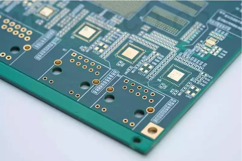
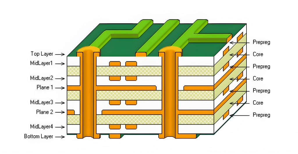
Multilayer PCBs are composed of three or more conductive layers. These layers are arranged in a stack with insulating layers (also known as dielectric layers) separating each copper layer. The number of layers can vary, with some advanced PCBs featuring more than 50 layers. The layers are connected through vias, which are tiny holes drilled through the PCB to provide electrical connections between different layers.
Common Applications
Multilayer PCBs are commonly used in applications that require a high degree of performance, miniaturization, and reliability, such as:
- Computers and Servers: High-speed data processing and transmission.
- Telecommunication Devices: Complex signal routing in smartphones and networking equipment.
- Medical Devices: Precision instruments that require compact and reliable PCBs.
- Military and Aerospace: High-performance electronics with strict reliability standards.
Key Considerations in Multilayer PCB Layout
Designing a multilayer PCB is a complex task that requires careful planning and consideration of several critical factors:
- Layer Stackup Design of multilayer PCB layout
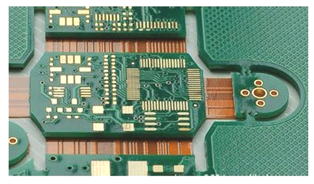
The layer stackup is the arrangement of conductive and insulating layers in the PCB. A well-designed stackup is crucial for ensuring signal integrity, controlling electromagnetic interference (EMI), and maintaining mechanical stability.
• Signal Layers: These are the layers where the actual circuitry is routed. In a typical stackup, the signal layers are interleaved with power and ground planes to minimize noise and crosstalk.
• Power and Ground Planes: These layers provide a continuous path for power and ground, reducing impedance and noise. They also act as a reference plane for signal layers, improving signal integrity.
• Prepreg and Core: These insulating materials separate the conductive layers and provide mechanical strength. The choice of materials affects the PCB’s dielectric constant, which influences signal speed and impedance. - Impedance Control of multilayer PCB layout
Impedance control is critical in multilayer PCBs, especially for high-speed digital and RF circuits. Controlled impedance ensures that the signal’s integrity is maintained across the PCB. Impedance depends on the width of the traces, the dielectric constant of the insulating material, and the distance between the traces and the reference plane.
• Microstrip and Stripline Configurations: These are common transmission line structures used in multilayer PCBs. Microstrip lines are on the outer layers with air as one of the dielectric mediums, while stripline configurations are embedded between two dielectric layers.
• Differential Pairs: For high-speed signals, differential pairs (two traces carrying complementary signals) are used. The spacing between the pairs must be tightly controlled to maintain impedance. - Via Design of multilayer PCB layout
Vias are essential for connecting different layers in a multilayer PCB. However, they introduce discontinuities in the signal path, which can affect signal integrity.
• Through-Hole Vias: These vias go through the entire PCB stack and connect all layers. They are simple to design but can introduce unwanted parasitic capacitance and inductance.
• Blind and Buried Vias: These vias only connect certain layers and are not visible from the outer layers. They are used in high-density PCBs to save space and reduce signal interference.
• Via-in-Pad: A technique where vias are placed directly under the pads of surface-mounted components, saving space and improving signal integrity. - Thermal Management of multilayer PCB layout
As devices become more powerful, managing heat in multilayer PCBs becomes increasingly important. Poor thermal management can lead to overheating and failure of components.
• Thermal Vias: These are vias that connect the thermal pads of components to inner layers or the opposite side of the PCB, allowing heat to dissipate more effectively.
• Copper Pour: A copper pour is an area of the PCB filled with copper, which can help spread heat and reduce the PCB’s overall temperature.
• Heat Sinks and Thermal Pads: In some cases, external heat sinks or thermal pads are required to manage heat effectively. - Signal Integrity and Crosstalk of multilayer PCB layout
Signal integrity refers to the quality of the electrical signals as they travel through the PCB. In multilayer PCBs, maintaining signal integrity is challenging due to the high density of traces and the complexity of the layout.
• Trace Spacing: Keeping adequate spacing between traces is essential to reduce crosstalk (unwanted coupling of signals between adjacent traces).
• Return Path: Ensuring that every signal has a clear return path to the ground plane minimizes the risk of signal reflection and noise.
• Terminations: Proper termination of signal lines, such as using resistors at the ends of traces, can reduce reflections and improve signal integrity.
Benefits of Multilayer PCBs
The complexity of multilayer PCBs offers several benefits that make them indispensable in advanced electronics:
- Higher Component Density
Multilayer PCBs allow for more components and interconnections in a smaller area. This is critical in modern electronics, where space is often limited. - Enhanced Performance
The use of multiple layers enables more sophisticated circuit designs, leading to improved performance, such as faster signal processing and better signal integrity. - Reduced Size and Weight
By stacking multiple layers, the overall size and weight of the PCB can be reduced, which is crucial for portable and wearable devices. - Improved Power Distribution
The use of dedicated power and ground planes allows for more stable and efficient power distribution across the PCB. - Better Signal Integrity
With controlled impedance and careful layer stackup design, multilayer PCBs offer better signal integrity, essential for high-speed circuits.
Challenges in Multilayer PCB Layout
Despite the benefits, designing multilayer PCBs comes with its challenges:
- Increased Cost
The complexity of multilayer PCBs makes them more expensive to manufacture than single or double-sided PCBs. The cost of materials, fabrication, and testing all contribute to the higher price. - Design Complexity
Designing a multilayer PCB requires a higher level of expertise. Engineers must carefully consider factors such as impedance control, thermal management, and signal integrity, making the design process more time-consuming. - Manufacturing Complexity
Manufacturing multilayer PCBs is more challenging due to the need for precise alignment of layers, accurate drilling of vias, and careful handling of materials. Any error in the manufacturing process can lead to costly rework or even complete failure of the PCB. - Difficulty in Testing and Repair
Testing and repairing multilayer PCBs can be challenging due to the complexity of the circuit and the difficulty in accessing inner layers. Specialized equipment and techniques are often required.
Best Practices for Multilayer PCB Layout
To successfully design and manufacture multilayer PCBs, following best practices is essential:
- Plan the Layer Stackup Early
Start by determining the number of layers and their arrangement based on the complexity of the circuit, signal integrity requirements, and thermal management needs. - Use Simulation Tools
Utilize simulation tools to analyze and optimize the PCB layout. Tools such as signal integrity simulators and thermal analysis software can help identify potential issues before manufacturing. - Maintain Consistent Trace Widths and Spacing
Ensure that trace widths and spacing are consistent across the PCB to maintain controlled impedance and minimize crosstalk. - Carefully Place Vias
Avoid placing vias in critical areas where they might introduce unwanted parasitic effects. Use blind and buried vias where possible to reduce the impact on signal integrity. - Collaborate with Manufacturers
Work closely with PCB manufacturers during the design process to ensure that your design is manufacturable and meets the required specifications. Discuss materials, layer stackup, and via design early in the process. - Perform Rigorous Testing
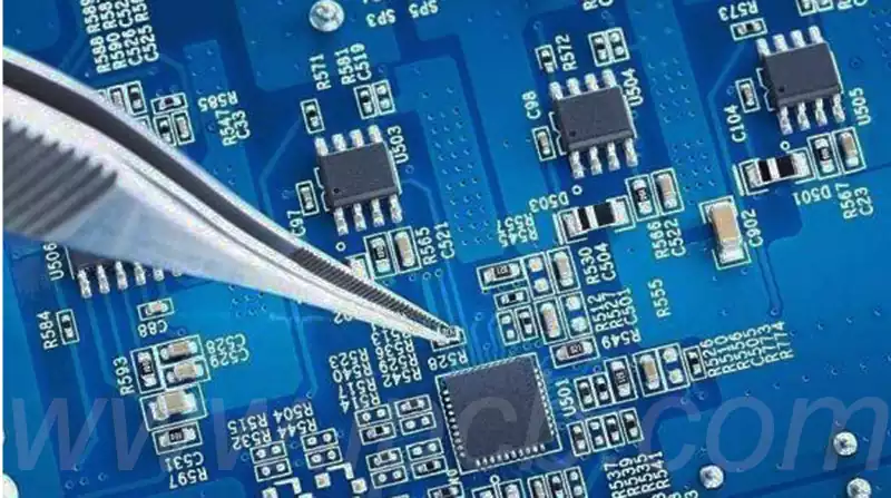
After manufacturing, perform rigorous testing to verify the PCB’s performance. Use techniques such as automated optical inspection (AOI), X-ray inspection, and electrical testing to ensure the PCB meets the design specifications.
Multilayer PCB layout is a complex yet rewarding endeavor that enables the creation of high-performance, compact, and reliable electronic devices. By understanding the key considerations, benefits, challenges, and best practices outlined in this article, designers can create multilayer PCBs that meet the demands of modern electronics. As technology continues to advance, the importance of multilayer PCBs in various applications will only grow. Therefore, staying updated with the latest design techniques and industry trends is essential for anyone involved in PCB design and manufacturing.