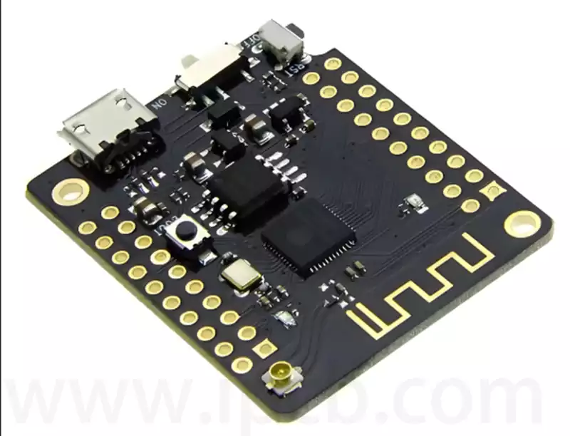
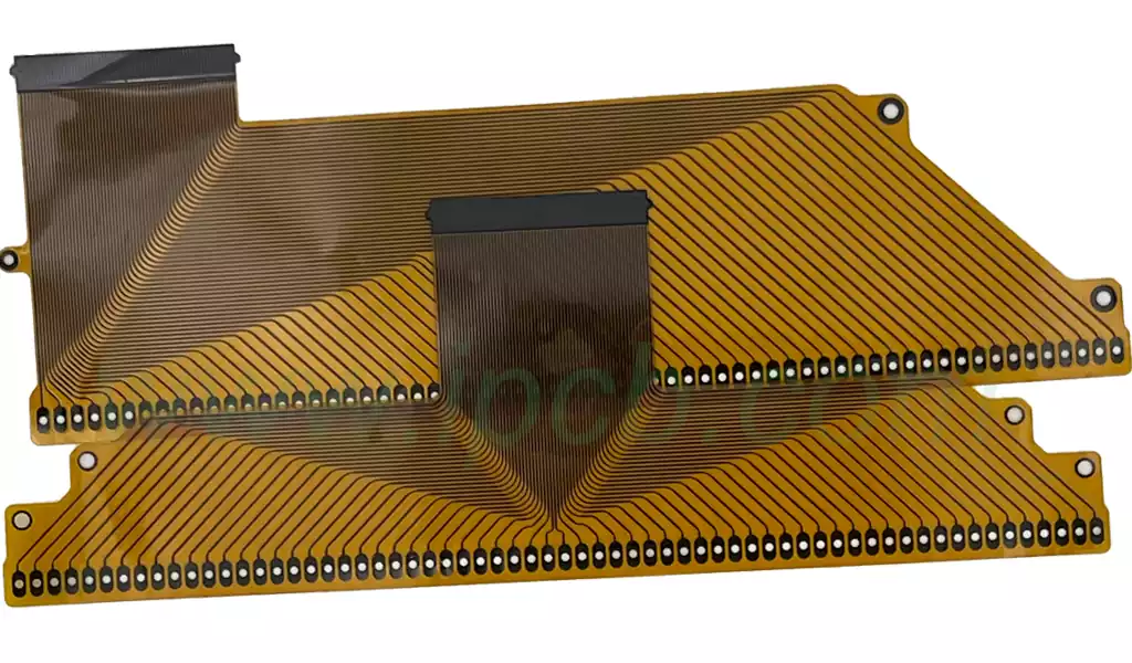
Heavy copper flex PCB refers to circuit boards with thicker copper layers in the flexible circuit board, which are usually between 100 and 400 microns thick, far exceeding the 35 micron copper thickness of standard PCBs. This design not only improves the current-carrying capacity of the board, but also greatly enhances its thermal performance. Flexible substrates are mostly made of polyimide (PI) or polyester (PET) films, giving the boards good bending, folding and three-dimensional spatial adaptability to meet the needs of complex assemblies.
Advantages of Heavy Copper Flex PCB:
Superior Electrical Performance
Copper as a conductor has very high electrical conductivity. The thick copper layer reduces resistance and signal attenuation during signal transmission, helping to maintain the integrity and stability of high-frequency signals, thus enhancing circuit performance.
Excellent Thermal Management
High frequency electronic components generate a lot of heat during operation. The thick copper layer and strong thermal conductivity of heavy copper flex PCB can quickly conduct heat away, avoiding performance degradation or damage due to overheating and improving the reliability and service life of the equipment.
Impedance Control of High Frequency Signals
Due to the good structural stability and material uniformity of heavy copper flex PCB, it can precisely control the impedance during design to ensure the precision and consistency of high frequency signal transmission, which is conducive to reducing signal interference and crosstalk.
Flexible Layout and Space Utilisation
Flexible substrates give PCBs excellent bending and folding properties to adapt to complex assembly spaces, which is particularly important for high-frequency communication equipment requiring compact, thin and lightweight design, which can effectively save space and enhance the overall performance of the system.
Mechanical strength and durability
Thick copper layer enhances the mechanical strength of the board, so that the heavy copper flex PCB can withstand vibration, shock and other harsh environments in high-frequency applications, to ensure the stable operation of electronic equipment.
Application areas of heavy copper flex pcb:
Power electronics and high power equipment
Due to its ability to carry high current, heavy copper flex PCB is widely used in battery management systems (BMS), inverters, high-voltage charging equipment, etc., especially in the field of new energy vehicles to show significant value.
Communication and High Frequency Electronics
The development of 5G and IoT devices puts higher requirements on transmission rate and signal stability, and the high-performance copper layer and flexible layout of heavy copper flex PCB provides support for high-speed signal transmission.
Medical and Military Equipment
High reliability and excellent thermal management make heavy copper flex PCBs suitable for medical monitoring equipment, military radar systems and other electronics in harsh environments.
Aerospace & Industrial Automation
In extreme environments, the mechanical strength and thermal stability of heavy copper flex PCB ensures safe and stable operation of equipment that meets the stringent standards of the aerospace and industrial sectors.
Common Challenges in Manufacturing Heavy Copper Flex PCBs
Thin and deformable materials
Flexible PCBs are usually only 0.05mm to 0.2mm thick, and the addition of a thick copper layer is more likely to lead to deformation of the board, affecting the accuracy of the laser drilling, exposure and etching processes.
High-precision line width/spacing requirements
High-end applications such as 5G communications require line widths/spacing of 30μm or even less, and the characteristics of the heavy copper material make ultra-fine lines difficult to process and prone to copper foil stripping or fracture.
Dynamic bending and reliability testing
Heavy copper flex PCBs need to withstand multiple bending and high temperature and humidity testing in complex environments to ensure their mechanical stability and electrical performance in use.
High Manufacturing Costs and Complex Processes
The manufacturing process involves multiple etching, precision lamination, and special fixtures for fixing, and the heavy copper layer makes the overall process complex and the costs rise significantly.
Difficulty in through-hole and via machining
Thick copper poses a challenge for etching and filling of through-holes, which is prone to side-etching and poor sealing of the through-hole, affecting the electrical connection and mechanical strength.
Solution:
Use specialised fixtures
Fix thin plates with flexible fixtures and vacuum adsorption equipment to reduce material deformation and improve drilling and exposure accuracy.
Advanced laser etching technology
Laser direct writing and etching ensures high precision formation of copper traces, reducing errors and side effects associated with traditional chemical etching.
Adoption of adhesive-free structural adhesive
Adhesive-free technology reduces interlayer thickness, enhances heat resistance and flexibility, and improves the mechanical properties of multilayer boards.
Multiple detailed etching and fluid circulation control
To reduce by-etching and over-etching, rapid etching methods are used and multiple fluid exchanges are used to reduce the degree of side-etching and ensure the shape of the copper layer is stable.
Dynamic Bending and Environmental Simulation Testing
Rigorous bending and aging testing processes are introduced into the design to ensure that the product can stably adapt to the actual usage environment.
Optimised through-hole filling technology
Conductive and non-conductive materials are used to seal through-holes, enhancing mechanical and electrical properties and avoiding rupture due to differences in coefficients of thermal expansion.
Material Optimisation and High Performance Substrate Selection
Selection of high-strength and high-temperature resistant PI substrates and rolled annealed copper improves the performance and reliability of the overall flex PCB.
Heavy copper flex PCB has become an indispensable key technology in many high-end electronic fields due to its excellent current-carrying capacity and outstanding thermal management performance brought by its thick copper layer, combined with the superior bending adaptability of the flexible substrate. In the future, with the continuous improvement of material performance and manufacturing process, heavy copper flex PCB will certainly promote the development of electronic products to higher performance, thinner, lighter, more compact and more durable, and help the electronics industry to move towards a more intelligent and diversified new era.