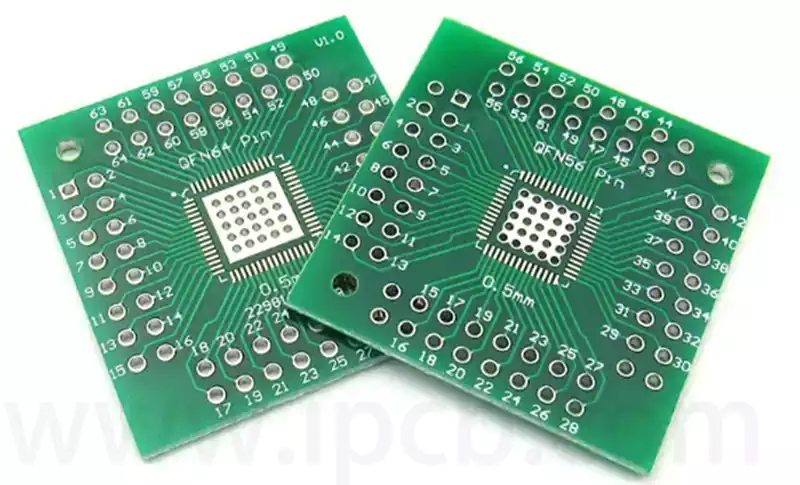
Low volume PCB assembly refers to the assembly and processing of circuit board components in relatively small quantity ranges. This type of assembly typically involves orders with lot sizes between 25 and 5,000 pieces and is suitable for product design phases that require flexible production and rapid iteration.
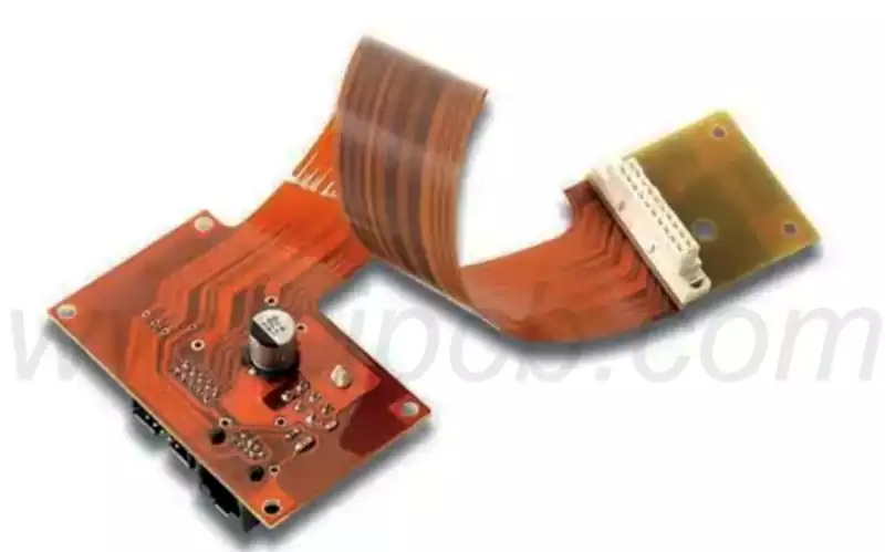
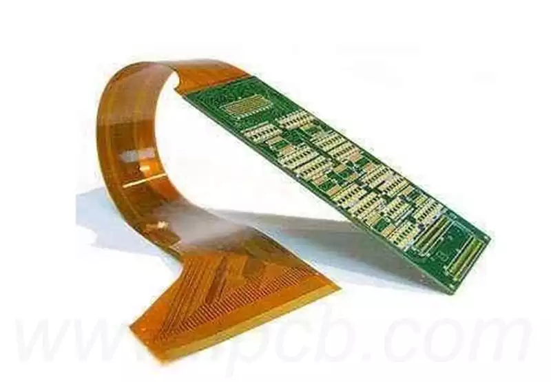
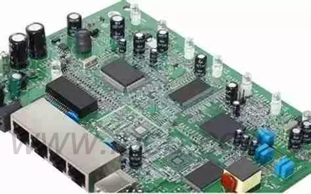
What is pcb assembly?PCB assembly (printed circuit board assembly) is a process of soldering or assembling electronic components onto a printed circuit board (PCB). This process, often abbreviated as PCBA (Printed Circuit Board Assembly), is a critical step in transforming an electronic design into an actual functional circuit.Through PCB assembly, electronic components and circuits can form complete electrical connections to realize the functions of various electronic devices.
The basic process of PCB assembly
1.PCB design creation
The first step in PCB assembly is to create a PCB design, which is usually accomplished through computer-aided design (CAD) software. The design concept includes circuit diagrams and component layouts to ensure proper placement of each electronic component on the board. When the design is complete, it is sent to a computer-aided manufacturing (CAM) system, which is used to generate the machining paths and instructions needed for manufacturing.
- Pattern Etching
After generating the processing paths and instructions, the next step is to etch the design onto the dielectric substrate. The etching process is usually performed using photochemical methods to ensure that the conductive paths are accurately formed. This phase is a critical step in ensuring that the circuit functions properly. - Component Placement
The next step is to place the electronic components onto the pads on the circuit board. This can be done manually or by automated equipment. Modern surface mount technology (SMT) allows the use of robots to efficiently and accurately place the components in their intended positions, reducing human error. - Soldering Process
Once all components are in place, soldering is performed to maintain a solid connection between the components. Soldering methods include reflow and wave soldering, where the solder melts and solidifies during the heating process to ensure a reliable electrical connection. The quality of the soldering process directly affects the performance and reliability of the final product. - Cleaning and Inspection
After the soldering is completed, the PCB usually needs to be cleaned to remove flux residues generated during the soldering process. This step helps prevent future failures and ensures the long-term stability of the board. Subsequent inspection sessions typically include visual and automated optical inspections to ensure solder quality and connection integrity. - Functional Testing
Finally, the fabricated PCB is subjected to functional testing to verify that it works as intended. During testing, power and analog signals are passed through the PCB to monitor electrical characteristics and ensure the reliability of the final product.
This approach is particularly well suited for prototyping, product testing, and small-scale marketing scenarios.Low volume pcb assembly offers significant cost advantages, especially in changing technology scenarios.
Companies can customize to specific needs without incurring the additional costs associated with mass production. The nature of small orders eliminates the need for companies to produce excessive quantities of boards, thereby reducing inventory risk and associated overhead. This approach is particularly well suited for product design validation or pilot programs in the R&D phase.
Small-lot production can respond quickly to changes in market demand, supporting rapid iteration and the flexibility to adapt designs. This flexibility allows companies to make quick adjustments in the face of new technological demands and market changes without having to worry about the fixed costs of high-volume production. In addition, it usually choose more diverse materials and components, which in turn promotes innovation.
Low volume PCB assembly is used in a wide range of applications including, but not limited to, consumer electronics, medical devices, robotics, and aerospace. Especially in medical equipment, due to the constant technological upgrades, the demand is often for specialized equipment in small batches with high precision, which provides a lucrative market space for low volume pcb assembly.
Low volume pcb assembly in the quality control of specific measures
- Welding quality control
In small batch PCB assembly, ensuring soldering quality is a critical step. Soldering temperature profiles and soldering times must be implemented correctly, and appropriate solder and soldering equipment must be used. This includes inspections for defects such as solder joint shape, solder pad coverage, and absence of solder bubbles and cold soldering to ensure the stability and reliability of the connection. - Component procurement and inspection
Component procurement is the basis for ensuring the quality of PCB assembly. In the procurement of electronic components, you need to order the required components in a timely manner and select a reliable supplier, check the specifications, packaging and quantity of components to avoid subsequent mismatch or out-of-stock problems. In addition, quality inspection should be conducted after procurement to ensure that all components meet the requirements. - PCB design verification
It is very important to perform PCB design verification before assembly. Ensure that the circuit diagram is consistent with the layout file, size, aperture and pads and other parameters are correct, can effectively reduce the subsequent assembly problems. This process should include design specification checks and design rule reviews to improve the manufacturability of the design. - Quality Inspection and Testing
Quality inspection and testing is necessary to ensure the quality of small batch PCB assembly. Visual inspection and automatic optical inspection (AOI) can be timely detection of components placed in reverse, leakage of solder, short circuit and other issues. In addition, functional testing or electronic testing to verify the performance and functionality of the PCBA board to ensure the reliability of the product in actual use. - Static electricity protection management
In small batch PCB assembly, managing electrostatic protection is an important measure to prevent electronic component damage. Appropriate anti-static equipment and workbench must be used, grounded to avoid static damage to components and circuits. This helps to improve overall assembly quality and reduce failures caused by static electricity. - Records and Traceability
Establishing detailed records, including information such as device lists, assembly process parameters and test results, allows for effective production traceability and problem identification. This step is an important part of the quality control system, helps in the emergence of problems for rapid response and improvement
The importance of PCB assembly as a key process for connecting electronic components to functional circuits cannot be overstated. Whether in traditional PCB production or in flexible small batch assembly, it is critical to ensure high quality soldering, component sourcing, design verification and quality testing, which not only affects the performance and reliability of the final product, but also determines the competitiveness of the company in the market.Low volume pcb assembly provides companies with the ability to respond quickly to changes, allowing technology iteration and product improvement to proceed smoothly, thus gaining more opportunities and room for innovation in the rapidly evolving electronics industry. With the diversification of market demand, the advantages of small batch PCB assembly will create outstanding market performance and technological breakthroughs for more enterprises!