Radio frequency circuit board plays a vital role in modern communication systems, especially in applications such as wireless communications,radar systems and medical devices. However, RF signals are susceptible to various types of interference during propagation, which can lead to signal distortion and system performance degradation. To ensure the reliability and stability of RF circuit board, it is particularly important to employ effective anti-interference design.
The first design responsibility is to carry out a detailed circuit analysis to identify the core circuit components. This involves identifying possible sources of interference and susceptible circuits, as well as thoroughly understanding the paths that interference can take to affect sensitive circuits. Given that RF circuits operate in the high-frequency range and rely heavily on electromagnetic radiation to cause interference,the core purpose of RF circuit board anti-interference design is to reduce the intensity of electromagnetic radiation from the PCB board and to reduce mutual interference between different circuits.
Radio frequency circuit board design
Component Layout
In view of the SMT (surface mount technology) commonly used infrared furnace thermal convection welding to complete the component bonding, the arrangement of the component configuration is directly related to the quality of the solder joints, which in turn has an important impact on the final pass rate of the product. In the scope of RF circuit board design, electromagnetic compatibility requires each circuit module as far as possible not to release electromagnetic radiation, and have a certain ability to resist electromagnetic interference. Therefore, the arrangement and configuration of components also profoundly affects the interference generation and anti-interference performance of the circuit itself, which is directly related to the functional performance of the circuit design. In the PCB design of RF circuit board, in addition to the need to take into account the layout of conventional PCB design considerations, but also need to think about how to weaken the mutual interference between the various components of RF circuits, as well as how to mitigate the interference of the circuit itself on other circuits and enhance the anti-jamming performance. The performance of RF circuits, not only depends on the performance indicators of the RF circuit board itself, but also by the interaction with the CPU processing board constraints. Therefore, in the PCB design, a reasonable layout of components is particularly important.
In the layout process should pay attention to is: the first step is clear and other PCB board or system connected to the interface components in the PCB board in the specific location, while the need to pay attention to the interface between the coordination of components.
In view of the small size of some electronic equipment, component layout closely, for the large size of the components, we need to give priority to be considered and determine its position, while taking into account the coordination between them.
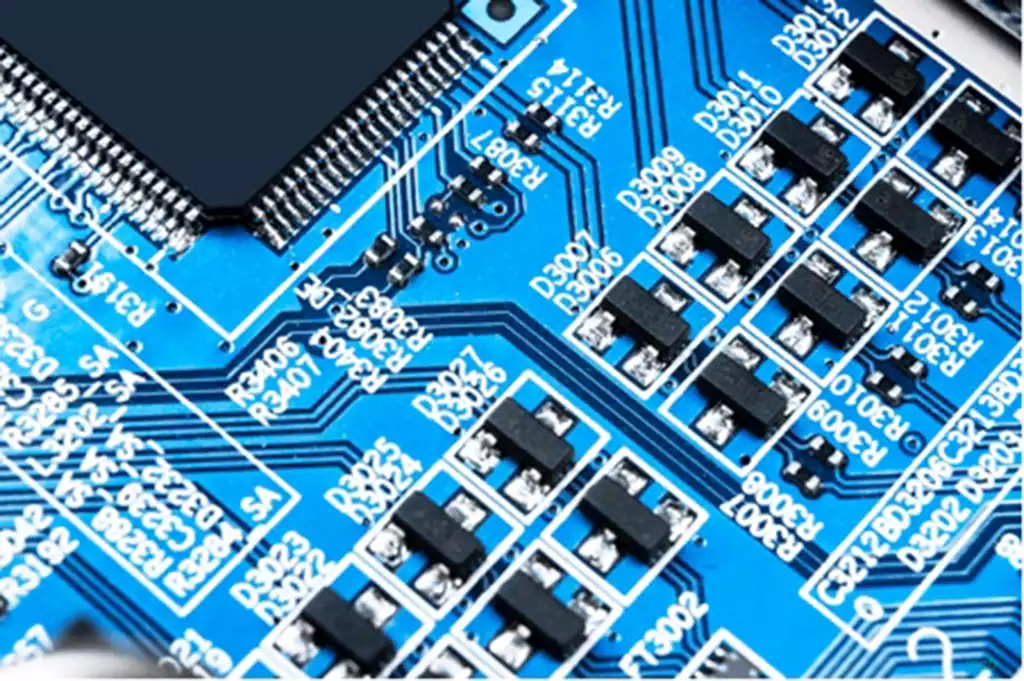
Analysis of the circuit architecture, the implementation of modular division of the circuit, such as: high-frequency amplification module, mixing module and demodulation module, etc., as far as possible to separate the strong electrical signals from the weak electrical signals, but also digital signal circuits and analogue signal circuits are laid out separately. Circuits performing the same function should be concentrated in a certain area as much as possible to reduce the area occupied by the signal loop. The filtering network of each circuit module should be connected in close proximity, so as to reduce both the radiation and the possibility of interference, thereby enhancing the anti-interference performance of the circuit.
Categorise unit circuits according to the differences in their sensitivity to EMC in use. For those parts of the circuit that are susceptible to interference, their components should be laid out as far away as possible from sources of interference, such as interference from the CPU on the data processing board and other factors.

Wiring
After the component layout is determined, the next step is to start wiring. The basic principle of wiring is to ensure that the assembly density meets the requirements of the premise, as far as possible, choose a low-density wiring scheme, and to ensure that the width of the signal line and the line spacing to maintain consistent, so as to facilitate impedance matching.
In RF circuits, improperly designed signal line routing, width and line spacing may cause cross-talk between signal transmission lines. At the same time, the system power supply itself will also bring noise interference. Therefore, when designing the rf circuit board, comprehensive consideration must be given to implementing a reasonable line layout. The power lines should be designed to be as wide as possible in order to reduce the loop resistance, and at the same time ensure that the direction of the power lines and ground lines is consistent with the direction of data transmission, thereby enhancing the anti-interference capability. Signal lines should be arranged as briefly as possible and the use of vias should be reduced. The shorter the connecting lines between components, the better, so as to lower the distribution parameters and reduce mutual electromagnetic interference. For incompatible signal lines, the distance should be maintained as far as possible to avoid parallel wiring, and the positive and negative signal lines should be perpendicular to each other. In the line layout, when encountering places that need to be turned, it is best to turn at an angle of 135°, avoiding the use of right-angle turns.
In the wiring process, the width of the lines directly connected to the pads should not be too large, and the alignment should try to avoid unconnected components to prevent short-circuit phenomena. Hole should avoid drawing on top of the components, and try to stay away from unconnected components to prevent quality problems such as false soldering, continuous soldering or short-circuiting in the production process.
In the rf circuit board design, the correct wiring of the power line and ground line is of vital importance, and reasonable design is a key means of eliminating electromagnetic interference. many sources of interference on the PCB are generated through the power supply and ground line, in which the noise interference generated by the ground line is particularly prominent. The reason why the ground line is prone to become the main source of electromagnetic interference is due to its impedance. When the current flows through the ground line, it will produce a voltage drop on the ground line, thus forming a ground loop current, triggering ground loop interference. When multiple circuits share the same ground, a common impedance coupling is formed, which in turn generates ground noise.
Therefore, in the rf circuit board ground wiring process, the following points should be noted:
When the modular division of the circuit, RF circuits can usually be divided into high-frequency amplification, mixing, demodulation, local oscillation and other major parts, for each of these circuit modules to provide a common potential reference point, that is, the independent ground of each module. Doing so ensures that signals can be transmitted smoothly between different circuit modules.
The digital and analogue areas should be separated as much as possible by ground lines, and the digital and analogue grounds should be separated and ultimately both connected to the power ground.At the same time,in the internal ground design of each circuit module,the principle of single-point grounding should also be followed in order to minimise the area of the signal loop and to ensure that it is connected to the ground of the corresponding filter circuit in close proximity.
If space conditions allow, it is best to isolate the ground line between the modules to prevent mutual signal coupling effects.
The core of the PCB design of RF circuits is how to reduce its radiation capacity and enhance its anti-interference capability.Reasonable layout and wiring is the key to ensure the quality of RF circuit PCB design.The above methods help to improve the reliability of rf circuit board design,effectively solve the electromagnetic interference problem, so as to achieve the design goal of electromagnetic compatibility.
Radio frequency circuit board anti-interference design requires comprehensive consideration of the layout and wiring,through the refinement of the design to reduce electromagnetic radiation and interference,to ensure the high performance and stability of the communication system,to meet the stringent requirements of modern electronic equipment.


