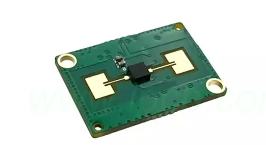
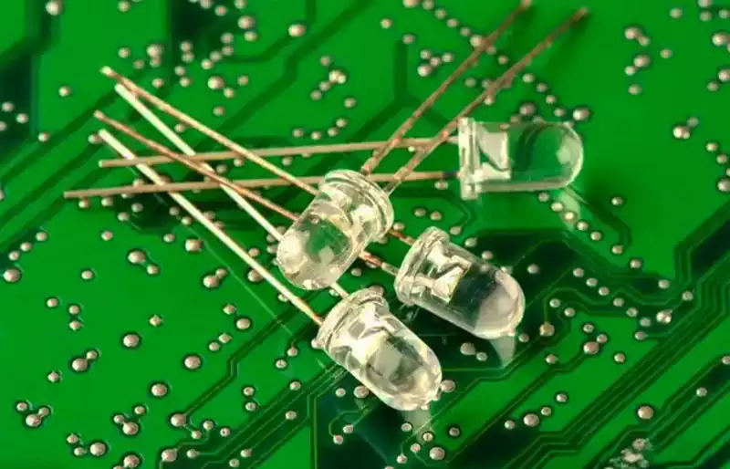
Optoelectronic circuit boards integrate circuits and optical components into a single unit, yet manufacturing such PCBs using existing processes presents significant challenges. 3D (additive) printing technology offers a novel approach for producing these boards, enabling smaller, lighter, and more intricate designs compared to traditional PCB fabrication methods, whilst consuming less power and generating lower pollution. Optoelectronic circuit boards also enhance electromagnetic shielding capabilities, enabling their use in boards with higher component densities.
Amidst the tide of technological advancement, semiconductor performance continues to escalate, with computational speeds accelerating relentlessly. Particularly within artificial intelligence and machine learning domains, the demand for computational power appears insatiable. Yet, as computational energy consumption rises, data transmission faces an increasingly urgent need for higher speeds. Against this backdrop, high-bandwidth applications undoubtedly represent the future trajectory for electronic components.
Achieving the throughput designed for faster chips necessitates communication channels with greater bandwidth. Yet enhancing throughput without increasing chip pin dimensions presents multiple challenges. On one hand, higher-frequency signal transmission generates additional interference and heat; while increasing pin counts (interconnections) not only drives up costs but also enlarges the physical footprint of electronic components.
The following explains why copper wiring cannot be further increased: copper is constrained by rise and fall times, with its capacitive and resistive characteristics preventing support for faster transmission speeds. Moreover, higher-frequency signal interactions generate stronger electromagnetic interference, while accelerated interaction frequencies lead to substantially increased power dissipation along the lines.
Attempting to boost throughput by increasing chip pin counts introduces a new set of challenges:
Packaging becomes larger and more costly;
Increased internal metal traces reduce yield;
Greater PCB area is required for routing;
Design complexity rises substantially;
Copper traces remain susceptible to electromagnetic interference.
In contrast, hybrid optoelectronic circuit boards offer an innovative solution. By embedding optical pathways to achieve higher-bandwidth communication, they overcome the aforementioned challenges while retaining copper for low-frequency signals. This unique design approach effectively enhances signal access speed and efficiency.
Application domains of optoelectronic circuit boards:
1.High-speed communications: Overcoming data transmission bottlenecks
Core applications: Within 5G/6G base stations, data centre server interconnects, and optical communication equipment, optoelectronic boards enable high-speed, low-loss data transmission via optical signals.
Technical advantages: Optical signal transmission remains unaffected by electromagnetic interference, reduces overall energy consumption by approximately 40% compared to purely circuit-based solutions, and supports transmission rates reaching several terabits per second.
Consumer Electronics Sector: Enabling Slimmer Designs and Enhanced Performance
Core Applications: Within compact products like smartphones, tablets, and wearables, optoelectronic circuit boards achieve high integration of optical paths and circuits through micro/nano fabrication.
Technical Advantages: Significantly improved structural compactness supports further device miniaturisation while meeting high-speed data transmission demands.
Industrial and Medical Sector: Ensuring Precise Control and Reliability
Core Applications: Within industrial automation equipment and medical electronic instruments, optoelectronic circuit boards deliver interference-resistant, highly stable signal transmission solutions.
Technical Advantages: Optical signal transmission remains immune to electromagnetic interference, ensuring precise device operation in complex environments.
Aerospace Sector: Conquering Extreme Environmental Challenges
Core Applications: In satellite communications and aircraft avionics systems, optoelectronic boards must withstand extreme conditions including vacuum, radiation, and extreme temperatures.
Technical Advantages: Utilising radiation-resistant materials and specialised encapsulation techniques ensures long-term stable operation.
Automotive Electronics Sector: Driving Intelligence and Electrification
Core Applications: Within intelligent driving systems and in-vehicle entertainment systems, optoelectronic boards support high-speed data transmission and low-latency control.
Technical Advantages: Wide operating temperature range (-40°C to 125°C) and vibration-resistant design adapt to complex automotive operating conditions.
Display Technology Sector: Enhancing Image Quality and Energy Efficiency
Core Applications: Within LCD and Mini LED display modules, optoelectronic circuit boards manage backlight control and signal distribution.
Technical Advantages: Optimises display performance through optical signal transmission while reducing energy consumption.
Optoelectronic hybrid circuit boards offer the following significant advantages:
Performance Leap
Thanks to the integrated design of electronic and optical components on a single circuit board, designers can flexibly select either optoelectronic chips or fully electronic chips within the same project based on actual requirements. In traditional configurations, fully electronic chips rely on copper wires for signal transmission, with each copper trace limited to a maximum bandwidth of approximately 40Gbps. In contrast, optical chips utilise embedded fibre optics for chip-to-chip interconnections, offering a substantial advantage in high-capacity bandwidth transmission. Specifically, fibre-based chip-to-chip communication achieves transmission speeds of 100Tbps or higher, representing a qualitative leap in data transfer performance.
Compact Dimensions
Optical waveguides are considerably slimmer than typical copper traces, with widths typically around 50μm. This characteristic enables optical waveguides to carry vastly greater data volumes within the same space as copper traces, theoretically exceeding copper by over 1000 times. Designers can leverage this advantage by replacing portions of copper wiring with optical fibres, effectively reducing circuit board dimensions. Furthermore, electronic and optical components no longer require separate boards but can be integrated onto a single circuit board. Additionally, the application of 3D printing technology enables optoelectronic circuit boards to create more complex and smaller structural features, further enhancing device density and accelerating information transmission speeds, with device density improvements approaching fifty percent.
Enhanced Energy Efficiency
Optical systems transmit information via photon propagation through fibres, whereas electronic systems rely on electron flow through conductors (typically metals). During operation, electron interactions in conventional electronics generate heat. If this heat is not effectively managed, system performance suffers significantly, and these interactions also induce additional interference. This explains why data centres invest millions of dollars in server cooling. By contrast, photonic devices and interconnects typically generate far less heat. This not only enhances device performance but also substantially reduces cooling costs.
Resistance to Electromagnetic Interference
Electromagnetic interference is a common phenomenon in electronic equipment, arising from the electromagnetic fields generated around circuits carrying current. These fields can penetrate various media, including air, and induce currents in nearby conductors – the fundamental principle behind radio operation. However, this electromagnetic field effect can induce currents in erroneous circuit paths, thereby disrupting data transmission and reception on normal lines. While most electronic designs can recover data from minor interference through coding techniques or meticulous copper routing, excessive electromagnetic interference on a single copper wire or channel can severely impair or even render it unusable.
Unlike copper wires, photonic waveguides remain unaffected by electromagnetic fields. Optical fibres themselves do not generate electromagnetic fields, even during high-frequency communication exchanges, nor are they affected by surrounding electromagnetic fields. Consequently, signal distortion is not a concern when transmitting data via fibre optics.
Hybrid optoelectronic circuit boards offer distinct advantages and immense potential. With ongoing breakthroughs in manufacturing technology and reduced costs, they are poised to make a significant impact in the electronic components sector, driving innovation and upgrades across multiple industries.