The audio ic board is one of the important components in the speaker equipment, and it undertakes many key functions. First, the audio IC board is responsible for receiving the signal from the audio source and converting the signal into current, then amplifying the current through the power amplifier part, and finally driving the speaker unit of the speaker to produce sound. Secondly, the audio IC board is also responsible for pre-processing the audio signal, such as equalizing and filtering the signal to obtain better sound quality. In addition, the audio circuit board can also provide a variety of connection interfaces, such as audio input, output, network interface, etc., so that users can easily connect and adjust the audio equipment.
The audio ic board is the core part of realizing the function of the audio equipment. It consists of multiple modules, such as signal input module, signal processing module, power amplifier module, etc. First, the signal input module is responsible for receiving and decoding signals from different audio sources, such as CD, DVD, Bluetooth, etc., and converting them into low-level analog signals. Next, the signal processing module will adjust and process the input signal, such as equalization, reverberation, delay, etc., to optimize the sound quality and sound field effect. Finally, the power amplifier module will amplify the processed signal and output it through the speaker to make the sound audible.
The working principle of the entire audio IC board involves the operation of multiple electronic components. For example, the signal input module uses a DAC chip to convert the digital audio signal into an analog signal, which is then amplified by an OP-AMP amplifier circuit. The signal processing module uses different circuits to implement various sound processing functions. The power amplifier module generally uses electron tubes, transistors or MOS tubes to amplify the signal. In addition, the audio circuit board will also be equipped with a power module, a clock module, etc. to provide power and precise clock signals.
What functions should the audio IC board PCB have?
These printed circuit boards have the following characteristics:
High input impedance
This feature is suitable for input signals, allowing the voltage to drop through the amplifier.
Low input impedance does not cause a voltage drop on the amplifier, so no signal is received.
This effect is why you should use low impedance materials to build the input.
In addition, high input impedance prevents loading, because low input impedance consumes a lot of current.
This effect causes loading on the circuit. In addition, this design will also minimize noise within the PCB.
High open-loop gain
This is the ability of the audio IC board to increase the amplitude or power of the signal.
When there is no feedback within the circuit, you can measure high open loop gain between the input and output ports.
High open loop gain allows for multiple levels of feedback and can achieve the right level of performance.
Limited Bandwidth
The audio IC board should be designed with the right bandwidth for the frequencies it amplifies.
Narrow bandwidth may result in some loss of signal frequencies, while wide bandwidth may introduce noise into the circuit.
Low Output Impedance
Once the voltage is reduced on the audio IC board PCB, it amplifies the signal.
Therefore, the impedance of the speaker should be higher than the impedance of the audio IC board PCB output.
Low output impedance results in a voltage drop across the speaker
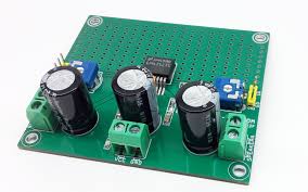
What should be considered when selecting audio IC board parts?
These include:
Dimensions
This is important throughout the stages involving drawing schematics.
Consider the following:
- Part connections
- Pins and outlines
- Case and packaging restrictions
- Top and bottom of the PCB
- Height clearance for polarized capacitors
Grounding Practices
Designing a proper grounding system requires planning from the conception of the design process.
Ensure there is an appropriate amount of ground planes and bypass capacitors.
In addition, decoupling capacitors are essential near the power to ground location.
The benefits of the ground plane include: - Shielding the circuit from noise radiated from the lower part of the PCB
- Improving the mechanical strength of the PCB
- Providing simpler circuit routing
- Adding distributed capacitance to minimize noise
- Allowing you to reduce impedance in the PCB, thereby reducing interference and noise
Distributing dummy components
It is important to design the BOM and then analyze the dummy audio IC board parts in the design.
Replace the parts that contain the package in the dummy part.
Spare gates
To prevent the spare gates from floating, connect them to the signal through their inputs.
This is important because floating inputs can interfere with the operation of the audio IC board.
Does the audio IC board have an offset voltage?
Correcting the input signal to achieve zero volts at the output of the audio IC board PCB is called the offset voltage.
In addition, you will also measure the offset voltage in the DC voltage.
Zero voltage at the input does not mean zero voltage at the output of the audio IC board PCB.
This is due to fluctuations and imbalances within the internal circuit units.
Therefore, adjusting the input helps you receive zero voltage at the output of the audio IC board PCB.
Input offset is the magnitude of the modification or correction you need.
The range of the offset voltage depends on the specifications of the board.
What are the applications of audio IC boards?
Audio IC boards operate in various systems as they help convert analog signals into digital signals.
They find applications in:
- Stereo systems
- TV audio
- Headphones
- Computer audio
- Car audio, etc.
What types of laminates can be used for audio ic board PCB?
Choosing the right laminate affects the stability, performance, power consumption, and assembly of the audio IC board PCB.
The laminates you can use include:
FR4
This is the most commonly used laminate in surface mount assembly.
FR4 has good strength-to-weight ratio, mechanical, physical, and electrical properties.
Also, it is flame retardant.
BT Epoxy
This laminate has high heat resistance, mechanical, and electrical properties.
Also, BT Epoxy is suitable for lead-free audio IC board PCB assembly and multilayer systems.
It can maintain adhesion at high temperatures, has high resistance to electromigration, heat resistance, and insulation.
High Tg Epoxy
This laminate is ideal for multi-layer audio IC board PCB.
It has excellent chemical and heat resistance, is versatile, flame retardant, and cost-effective.
In addition, it also operates effectively in applications with high humidity and temperature.
Polyamide
This laminate has high circuit trace bonding toughness and remains stable in extreme environments.
In addition, they are suitable for producing high-density audio IC board PCB.
In addition, they also have suitable thermal, mechanical, and thermal properties.
What is the purpose of heat sink in audio IC board PCB?
Heat sink helps to dissipate heat when audio IC board PCB is working.
In addition, aluminum material is suitable because it has high conductivity and can resist corrosion and wear.
It works with the help of copper traces and thermoelectric vias, and the working principles include radiation, conduction, and convection.
What is the chemical property of audio IC board?
Chemical properties include:
Flammability Specifications [UL94]
The Flammability Safety Standard for Plastic Materials for Parts of Equipment and Appliances [UL94] will rate the flame retardant properties of the plastic.
It states that the material needs to burn for less than 10 seconds when flammable.
Methylene Chloride Resistance [MCR]
This is the ability of the PCB to resist a chemical that checks the dielectric’s resistance to absorption of methylene chloride.
The MCR for dielectrics is between 0.01% and 0.20%.
Moisture Absorption
This is the ability of the PCB dielectric material to resist moisture in the presence of liquids.
Most PCB materials have moisture absorption rates between 0.01% and 0.20%.
Audio ic board design tips
Component layout
First, the general layout principle: components should be arranged in the same direction as much as possible, and the phenomenon of poor soldering can be reduced or even avoided by choosing the direction in which the PCB enters the tin melting system; it is known from practice that there must be at least 0.5mm spacing between components to meet the tin melting requirements of components. If the space of the PCB board allows, the spacing between components should be as wide as possible. For double-sided boards, one side should generally be designed for SMD and SMC components, and the other side for discrete components.
- Divide the PCB into digital and analog areas
The first step in any PCB design is of course to choose the PCB placement of each component. We call this step “board layout consideration”. Careful component layout can reduce signal interconnection, ground line segmentation, noise coupling, and the area occupied by the circuit board.
Electromagnetic compatibility requires that each circuit module should not generate electromagnetic radiation as much as possible and have a certain anti-electromagnetic interference capability. Therefore, the layout of components also directly affects the interference and anti-interference capabilities of the circuit itself, which is also directly related to the performance of the designed circuit.
Therefore, in addition to considering the layout of ordinary PCB design when designing RF circuit PCB, it is also necessary to consider how to reduce the mutual interference between the various parts of the RF circuit, how to reduce the interference of the circuit itself to other circuits, and the anti-interference ability of the circuit itself.
From experience, it is known that the effect of RF circuit depends not only on the performance indicators of the RF circuit board itself, but also on the mutual influence between the CPU processing board. Since RF circuits contain digital circuits and analog circuits, in order to prevent digital noise from interfering with sensitive analog circuits, the two must be separated. Dividing the PCB into digital and analog areas helps improve this type of
circuit layout, which is particularly important.
*It is necessary to prevent RF noise from coupling to audio circuits
Although the RF part of handheld products is usually treated as an analog circuit, a common problem that needs to be paid attention to in many designs is RF noise. It is necessary to prevent RF noise from coupling to audio circuits because RF noise generates inter-noise after demodulation. In order to solve this problem, the RF circuit and the audio circuit need to be separated as much as possible. After dividing the PCB into analog and digital, it is necessary to consider the component layout of the analog part. The component layout should make the path of the audio signal as short as possible. The audio IC board should be placed as close to the headphone jack and speaker as possible to minimize the EMI radiation of the Class D audio IC board and the coupling noise of the headphone signal. The analog audio signal source must be as close to the input of the audio IC board as possible to minimize the input coupling noise. All input leads are an antenna for RF signals. Shortening the lead length helps reduce the antenna radiation effect in the corresponding frequency band.
In short, audio ic boards and audio circuit boards are both indispensable parts of audio equipment. They bear the key function of converting audio signals into audible sounds, and can also improve sound quality and sound field effects through functions such as signal processing and enhancement. Understanding the role and principle of speaker circuit boards and audio circuit boards will help us better select and use speakers and audio equipment and enjoy high-quality music and sound experience.
