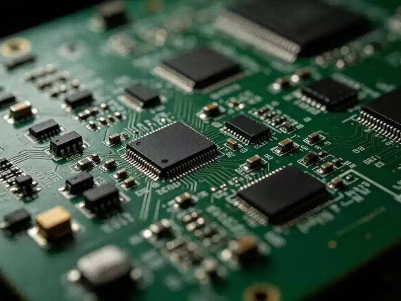
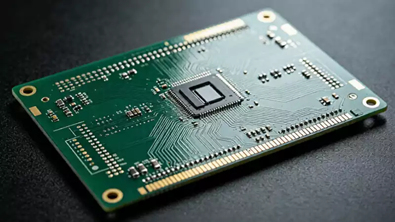
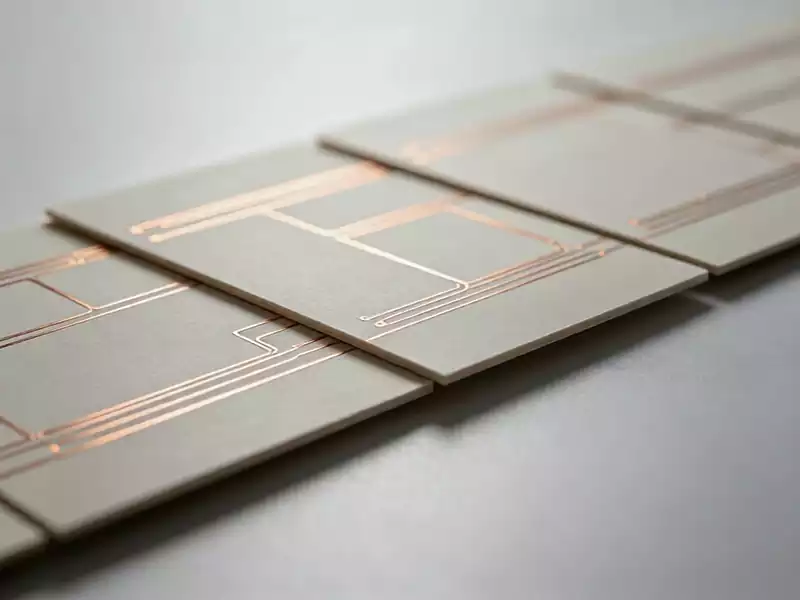
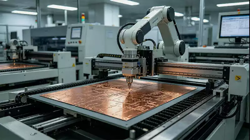
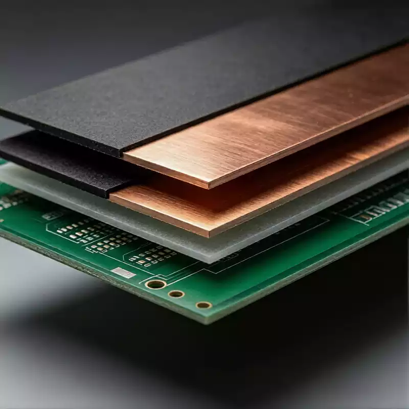
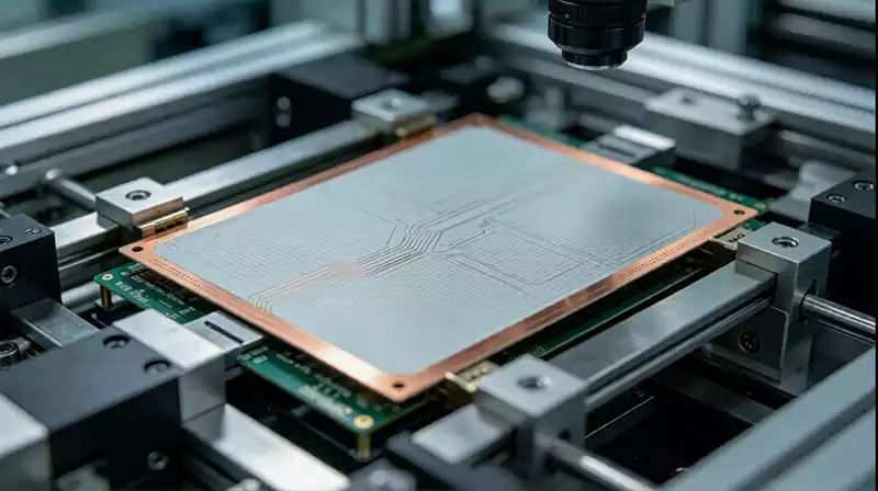
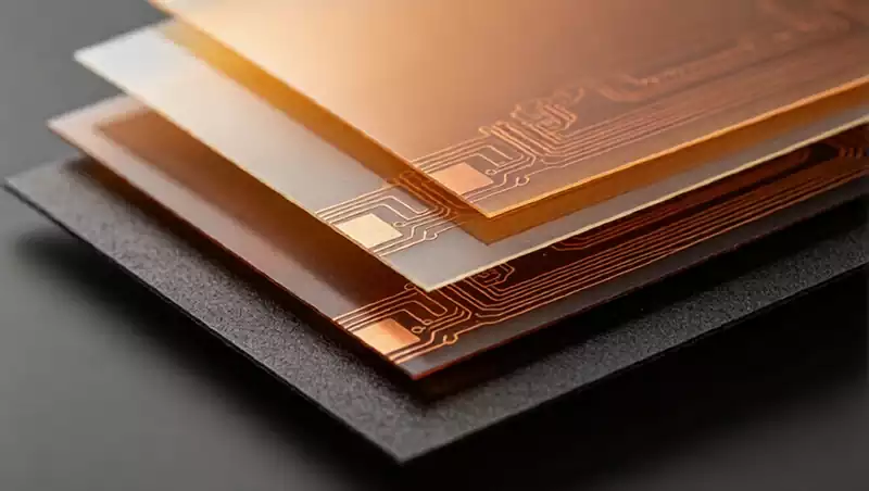
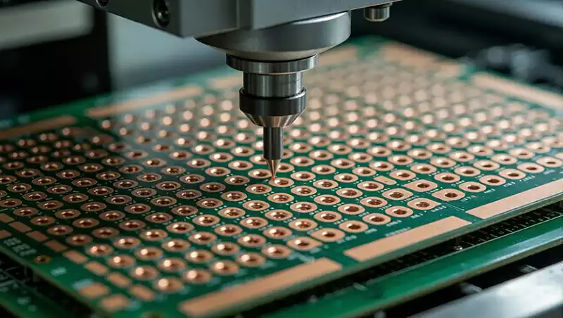
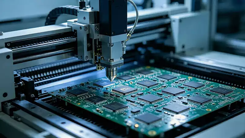
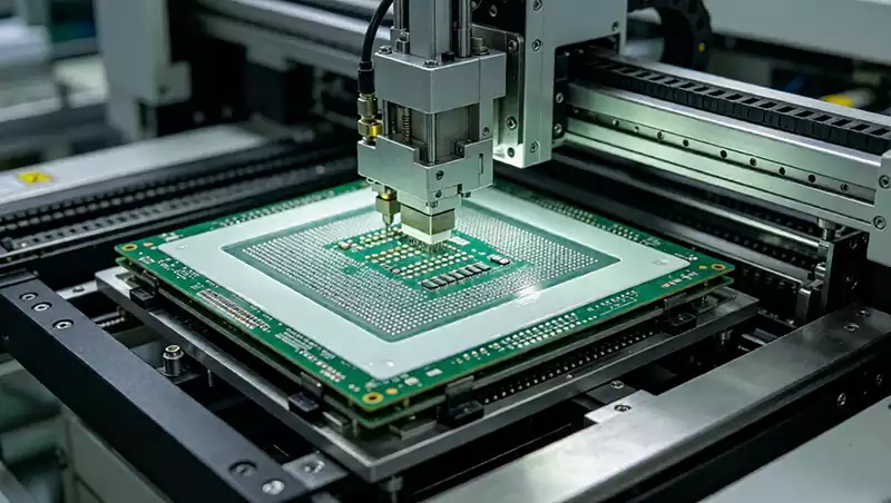
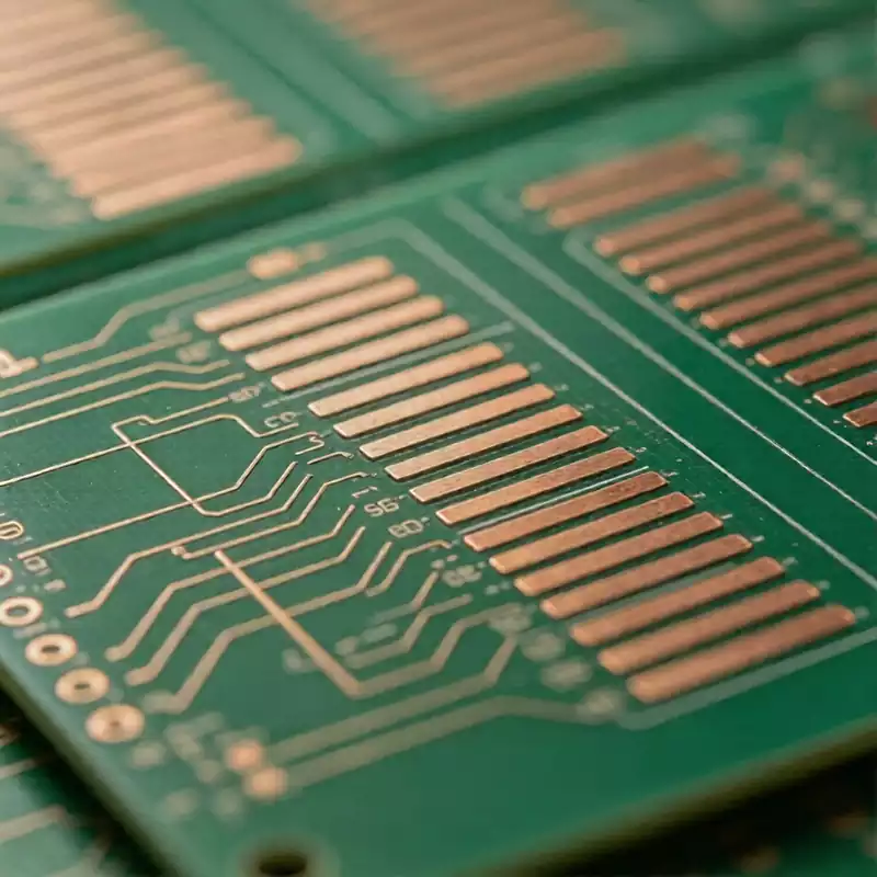
Electronic manufacturer

transparent flexible PCB

Future challenges and application for transparent flexible pcb

A transparent flexible PCB is a pcb board that can be bent and has a certain degree of flexibility without affecting its functionality. It is made of flexible materials such as polyimide or polyester film, allowing for compact circuit connections in a given space. Transparent flex pcb is lightweight and durable. It is this property […]

flexible circuit board

Key points and strategies for soldering flexible circuit board

FPC flexible circuit board is widely used in modern electronic products due to their thin, lightweight and bendable characteristics. However, its unique physical properties also bring many challenges to the welding process, requiring fine process control and specialised coping strategies. Flexible circuit boards in the welding process should pay attention to: Quality inspection is a

flex board

Deformation and Delamination Prevention in Flex Board Manufacturing

In the production of flex board, material deformation and delamination are important factors affecting product quality. In order to avoid such problems, the following detailed coping strategies can be adopted: Substrate selectionThe choice of material directly determines the basic bending performance of flex board. In terms of substrates, polyimide (PI) and polyester (PET) are commonly

high speed digital pcb

Key considerations and applications for high speed digital pcb

High speed digital pcb is circuit boards that can support high speed digital signal transmission, and are usually used in scenarios where the frequency of digital logic circuits reaches or exceeds 45MHz-50MHz, or where the delay of digital signals in circuits on the transmission line is greater than 1/2 rise time. Compared to traditional analogue

leadless chip carrier

Differences between leadless chip carrier and leaded chips

Leadless chip carrier refers to a chip substrate material that does not contain lead. Traditional chip carriers often use leaded materials because leaded materials have high plasticity and are easy to process during manufacturing, but leaded chips are harmful to the environment and the human body. Leadless chip carrier is widely used in the manufacture

pcb board assembly

Common defects in pcb board assembly processing

PCB board assembly processing, there may be a variety of defects, these defects can be categorised as the following major aspects, designed to improve product quality and reduce the defective rate. Welding defectsWelding is a key part of PCB board assembly processing, common welding defects include: False soldering (Dry Joints/Cold Solder): refers to incomplete solder

AMB ceramic substrate

Technology and Challenges of AMB Ceramic substrate

Ceramic substrate in accordance with the process points there are many kinds of, in addition to direct bonding copper (DBC) method, direct copper plating (DPC) method, laser activated metal (LAM) method, low-temperature co-fired ceramics (LTCC), high-temperature co-fired ceramics (HTCC) in addition to the AMB method of the technology that currently attracts much attention, that is,

chipset

What is a chipset and what does it do?

What is a chipset? A chipset is a processor that consists of multiple chips. Each chip in a chipset may be produced by a different manufacturer. These individual chipsets are combined together to form a processor using a complex connection system. Chipset processors can take advantage of the latest chip manufacturing technology to reduce the

ceramic substrates

Comparison of ceramic substrate and normal pcb

Ceramic substrates and PCBs play an important role in the electronics industry, each with unique material properties, manufacturing processes and application areas. Ceramic substrate is a ceramic material made of electronic substrates, belonging to the inorganic materials, usually with alumina (Al2O3), aluminium nitride (AlN) and silicon nitride (Si3N4) as the main component, ceramic substrate has

dip

What is dual inline package?

What is dual inline package? Dual inline package (DIP) is a type of integrated circuit package whose main feature is that the integrated circuit chip is mounted on two parallel rows of metal pins. This type of package is simple, easy to produce and maintain, so it is widely used in the electronics industry. Dual

ball grid array socket

Production considerations for ball grid array socket design

The ball grid array socket is an adapter that allows for pluggable mounting without directly soldering BGA-packaged integrated circuits (ICs) to the test substrate. By connecting the solder balls of the IC to the pads of the test substrate via the BGA socket, the risk of poor contact (e.g. open or short circuit) and IC

camera pcb board

Camera pcb board design

The design layout of a camera pcb board is a central aspect of ensuring camera performance, reliability and stability. An optimised layout can effectively reduce signal interference, improve signal integrity, and improve thermal management. Camera PCB Board Wiring GuideThe LVCMOS signal alignment needs to be away from the differential lines to prevent the LVCMOS line

camera pcb board

Introduction to Camera PCB Board

The camera motherboard, also called the camera pcb board, is one of the core components inside the camera and contains the camera’s processor. Memory. Interface chip. Sensor control chip and other important components. The role of the camera motherboard is to control and manage the various functions and operations of the camera, so that the

hybrid bonding

Process Principles and Development of Hybrid Bonding Technology

Hybrid Bonding is an advanced IC packaging technology used to achieve high-density, high-performance interconnections between different chips. The key feature of this technology is to replace the traditional bump or solder ball (bump) interconnections with direct copper-to-copper connections, which enables ultra-fine pitch stacking and packaging in a very small space for the purpose of three-dimensional

hybrid bonding

Hybrid bonding technology process and application

Hybrid bonding is an emerging packaging technology that combines the features of inter-chip bonding and intra-chip bonding. It utilises different bonding techniques to achieve interconnections between wafers and package substrates or within wafers to meet the needs of high-performance integrated circuits with complex interconnect structures. There are two common types of hybrid bonding: W2W can

FPC Bonding

FPC Bonding Technology Process

FPC Bonding (Flexible Printed Circuit Board Bonding) is a technology that electrically and mechanically connects flexible circuit boards (FPC/FPCB) to other electronic components, rigid circuit boards (PCBs), or components such as displays through a specific process. This process is widely used in consumer electronics (e.g., mobile phones, tablets, wearable devices), automotive electronics, and medical devices

differential signal

Differential Signal Cabling Design and Optimisation

Differential signal line is mainly the difference between the traditional signal line corresponds to a ground line signal transmission mode, differential signal transmission is mainly two lines on the signal transmission, the two signals are equal in amplitude and opposite in phase. Relative to the traditional single-ended signal, it has a strong anti-jamming, can effectively

flex pcb assembly

FPC PCB Assembly Process

There is a significant difference between FPC PCB assembly and the assembly of rigid circuit boards, the main reason is that flex board is softer and less hard, if you do not use a special carrier board, it is difficult to achieve effective fixation and handling, so as to be unable to complete the printing,

radar pcb

Radar PCB and their high frequency applications

Radar PCB is an RF circuit board used for detection and automation that is primarily responsible for generating, transmitting and receiving RF signals. It contains an antenna structure mounted on a high frequency laminate that transmits the radar flaps generated by the RF circuitry and receives the reflected radar pulses after hitting an object, which

PCB radar

PCB Radar Design Considerations

A PCB radar is a type of printed circuit board designed for use in radar systems and is primarily responsible for generating, transmitting and receiving RF signals. It is typically made of a high frequency laminate material that integrates an antenna structure for transmitting and receiving radar waves. The radar PCB is able to send

pcb substrate

PCB manufacturing process pcb substrate problems and solutions

As an important basic component of electronic products, the stability of pcb substrate dimensions during the manufacturing process of printed circuit boards directly affects the performance and reliability of the final product. However, substrate dimensions often change due to a variety of factors during the production process, resulting in dimensional deviations, bending and warping, and

multilayer circuit board

Manufacturing difficulties and solutions for multilayer circuit board

As a core component carrying complex functions and high-density interconnections in modern electronic products, multilayer circuit board faces many technical challenges in the manufacturing process due to their increased thickness, increased number of layers, and dense wiring and perforations. With the increasing demand for high-performance PCBs in fields such as 5G communications, artificial intelligence and

pcb dielectric thickness

PCB Dielectric Thickness Analysis

PCB dielectric thickness is usually the thickness of the glass fibre cloth or other special material used to cover both sides of a printed circuit board (PCB) during the manufacturing process. The choice of dielectric thickness depends on the specific application scenario and requirements of the circuit board. Multilayer board dielectric thickness refers to the

pcb thickness tolerance

PCB thickness tolerance and influencing factors

PCB thickness tolerance refers to the difference in the thickness of a circuit board due to the production process and equipment conditions during the manufacture of the pcb circuit board, which is the thickness tolerance of the board. This tolerance range depends mainly on the type and specification of the board used. Normally, the pcb

Scroll to Top