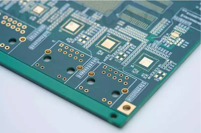
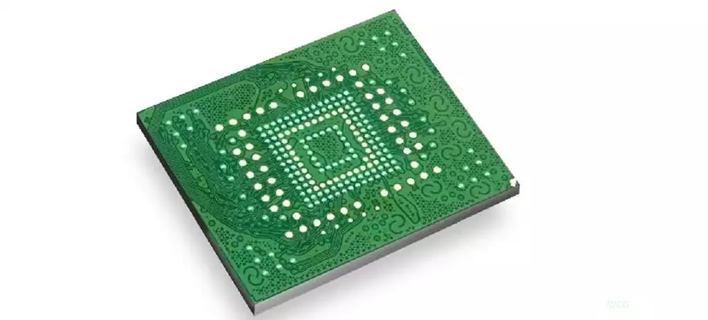
What is bga? BGA meaning Ball Grid Array Package, known as Ball Grid Array, is a surface mount packaging technology for integrated circuits. Its pins are arranged in an array on the bottom of the package substrate, and ball contacts are made as pins to connect with the printed circuit board (PCB).
BGA encapsulation process is divided into the front-end process and the back-end process, the specific flow is as follows
1) Wafer thinning:
The wafer thinning process is carried out on the backside of the wafer by high-speed rotary grinding with an abrasive wheel, while water cooling and cleaning measures are used to prevent high-temperature accumulation and debris buildup. When a chip needs to be a specific thickness, it is polished to remove internal stresses depending on the product type. After thinning is completed, tape is used to remove the lamination from the surface of the wafer, followed by thickness measurement and quality inspection.
2) Chip cutting:
After the wafer is thinned, a blue film is used to secure the wafer to a metal ring, and it is separated into individual chips by cutting technology. Currently, there are two main ways of blade cutting and laser cutting. Blade cutting utilizes a circular blade that cuts completely through the cutting channel, dividing the wafer into individual chips and arranging them in an orderly manner on the blue film. Laser dicing, on the other hand, utilizes the energy of the laser beam to evaporate the substance on the cut channel to achieve the separation of the wafer. With the development of IC wafer process to below 10nm, laser cutting is widely used due to its advantages such as no external force, small cutting width and high cutting quality.
3) Chip Mounting:
Chip mounting process is based on the design drawings using silver glue, DAF film and other patch materials to fix the chip on the substrate, its main role is to stabilize the chip and conduct the heat generated by the chip.
4) Plasma cleaning:
Before welding line and plastic sealing, plasma cleaning using ionized argon ions, electrons and active groups, so that the substrate and the chip surface pollutants into volatile gases, discharged through the vacuum system, thus cleaning the surface and improve the bonding force when welding line. Plastic sealing before the plasma cleaning principle is similar, aimed at removing surface contaminants and carbide, activation of the substrate surface, enhance the bonding force between PCB and plastic sealing material to improve product reliability.
(5) lead soldering:
Leads welding is a key part of the packaging process, through the welding of welding wire (such as gold, copper or silver alloy wire) and aluminum pads on the chip and the substrate metal pads connected to achieve electrical conduction.
6) Plasticizing:
The plastisol process begins with melting the plastisol into a low-viscosity liquid at high temperature and then injecting it into the mold cavity. Under the action of hardener, coupling agent and other additives, the epoxy resin inside the plastic sealing material is gradually cured to complete the plastic sealing.
7) Post-curing:
Post-curing stage in the high-temperature conditions of the plastic sealing material after the curing process. As the sealing material may not be fully reacted at the end of the sealing, it is necessary to promote its complete reaction by baking at high temperature to stabilize the molecular structure of the epoxy resin, enhance the hardness of the sealing body and eliminate internal stress.
8) Marking:
The marking process involves ink printing or laser engraving on the front side of the chip to mark the product name, production date and other information on the surface of the product to facilitate product identification and traceability.
9) Planting ball:
Fluxing is a special process for BGA packaging that involves printing flux and placing solder balls on the solder ball payoff pads (e.g. NiAu or copper-plated OSP antioxidant treatment) on the back of the substrate. Through the reflow furnace so that the tin ball melting, and the solder ball payment pad to form a eutectic, after cooling, fixed on the back of the substrate, after the completion of the reflow of the solder ball as a BGA package I / O external pins, to achieve the connection between the chip and external circuits.
(10) Cutting and sorting:
Cutting sorting is the whole BGA substrate products by cutting or stamping way to split into individual BGA chip process, this step marks the formation of the final product. Prior to this, the process is carried out in strips.
Characteristics of BGA
BGA encapsulation technology uses spherical solder joints to connect the chip and PCB substrate. Compared with the traditional QFP, SOP and other encapsulation methods, BGA has the following characteristics:
- High-density: BGA packaging method can realize the high-density layout of chip pins, so that the number of chip pins can be effectively improved.
- High speed: BGA package can realize the short path layout of chip pins, thus reducing the time delay of signal transmission and improving the working speed of the chip.
- High reliability: BGA package uses spherical solder joints to connect the chip and PCB board, the strength of the solder joints is higher than the traditional pad connection, with better resistance to vibration, shock, thermal expansion and other properties, which can improve the reliability of the chip.
- Small size: BGA package can realize the compact layout of chip pins, thus reducing the size of the chip.
Disadvantages of BGA package
Difficult to inspect
Although soldering helps to improve the performance of the package and the circuit as a whole, it is not without its drawbacks, the main problem being that once the package is soldered to the board it cannot be inspected. As a result, identifying any potential faults and fixing them can be difficult as it is not possible to look at the surface in the same way as with a PGA package. To counteract this package density, the likes of X-rays and CT scans are used to check for any aberrations in circuits or connections, although the process is expensive.
A bit pricey
While there may be IC packaging solutions that may cost less, using BGA packages is relatively expensive. For example, the bumping process and substrate are cost-adding factors compared to QFN packages.
BGA packaging technology has become one of the most important technologies for surface mount packaging of integrated circuits with its unique spherical solder joint connection, which enables high density, high speed, high reliability, and small size of chip pins. Through a series of delicate process steps, such as wafer thinning, chip cutting, chip placement, plasma cleaning, lead soldering, plastic sealing, post-curing, marking, ball-planting, and cutting and sorting, it ensures a stable connection and excellent performance between the chip and PCB. However, this technology also has challenges such as difficult inspection and high cost, which need to be overcome by advanced inspection technology and cost control means.