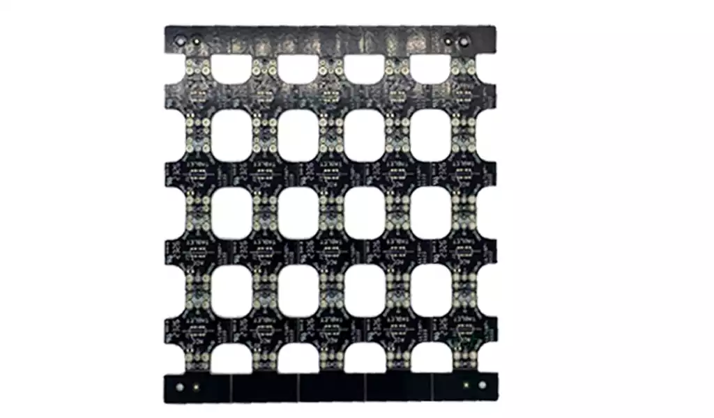
BGA Test Fixture (Ball Grid Array Test Fixture) is a test tool for testing BGA chips, which can provide electrical test, signal acquisition and programming functions for the chip. In the design of the BGA test frame, you need to consider the PCB (Printed Circuit Board) with the design, because the layout of the PCB and the connection will directly affect the accuracy and efficiency of the test.
The relationship between the design of BGA test stands and PCBs.
Precise correspondence between BGA test and pads: When carrying out BGA test, the test fixture and PCB pads need to be accurately matched. In the process of designing the BGA test frame, it is necessary to ensure that the probes on the test fixture can be accurately aligned with the pads of the BGA chips on the PCB, so as to ensure the high quality of signal transmission.
PCB Layout and Test Point Setting: During the PCB design phase, the reasonable layout of the test points should be fully considered. It is necessary to ensure that the probes of the BGA test frame can easily reach each test point, thus ensuring the comprehensiveness and accuracy of the test work.
Optimise the signal transmission path: PCB design needs to pay attention to the planning of the signal transmission path, should try to shorten the length of the path and ensure its stability, to effectively avoid signal interference and attenuation, and then ensure that the test results are accurate.
Scientific planning grounding design: PCB design process, grounding design is a key link. It is necessary to ensure that the grounding design is scientific and reasonable, to prevent the ground loop is too large or ground isolation phenomenon, so as not to adversely affect the signal quality and test results.
PCB Material Parameter Adaptation Test: The selection of PCB materials has a significant impact on the test results. When selecting materials, it is necessary to comprehensively consider the dielectric constant, thermal expansion coefficient and other key parameters to ensure that the selected materials can meet the test requirements for stability and reliability.
Reasonable design of through-hole layout: PCB design requires careful planning of the location and size of the through-hole. Reasonable through-hole design can facilitate the connection of test fixtures and ensure a smooth and unobstructed test process.
Strengthen PCB quality control: PCB design quality is directly related to the accuracy and reliability of BGA testing. Therefore, the PCB manufacturing process and quality standards must be strictly controlled to ensure the test quality from the source.
Dynamically optimize the design scheme: During the PCB design process, the design scheme should be adjusted and optimised in a timely manner in line with the actual test requirements and feedback information, so as to improve the test efficiency and accuracy of the results.
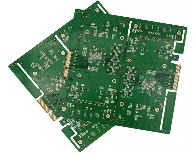
Process capability of PCB design for BGA devices
When designing PCBs containing BGA devices, in addition to the technical and functional aspects of the design, it is also necessary to communicate with the corresponding PCB manufacturing plants that have this processing capability. Including the manufacturing process and the corresponding cost. Different processing technology will affect the future mounting difficulty, product yield.
Processing technology, laser blind hole process need to do VCP side spray pulse plating copper to fill the blind holes, grinding to do negative acid etching to ensure the integrity of the BGA, etching the final size of the BGA in the final size of 0.27mm ~ 0.28mm. In addition, due to the BGA pitch is small, the processing process needs to pay attention to:
- Engineering design of the BGA compensation processing to ensure that the final pad requirements;
- Soldermask window, to ensure that the window can not be on the BGA pad, otherwise affect the mounting;
- The choice of ink, because the pitch is relatively small priority to choose high viscosity green ink;
- The choice of surface treatment process, usually BGA encapsulated PCB surface treatment selection of relatively flat surface treatment process, in order to ensure that the back of the chip tin ball and the best mounting effect of the PCB board;
Surface process: hot air levelling, immersion gold, silver, tin, OSP and other surface processes, OSP flux is the most superior, but need to pay attention to the protection of the oxide film is not oxidised and wiped flowers, PCB surface treatment to do the OSP required to be done within 3 months after the posting, otherwise it affects the welding. Cost OSP surface treatment process is relatively low processing costs.
In the PCB design process, for BGA chip wiring work, there are some widely used general skills. Among them, clear design rules is the first task, which covers the number of layers of the board, the minimum alignment width, alignment spacing and through-hole size and other key parameters. Generally speaking, the more layers of the board, the more room for manoeuvre and flexibility of the wiring, the wiring is correspondingly difficult to reduce, but at the same time will bring about an increase in manufacturing costs.
In addition, the expected output of the product is also a consideration that should not be ignored. For mass-produced products, in order to effectively spread the cost of each PCB, it is necessary to invest in detailed wiring work; for low-volume production of products, due to limited production, it may not be worthwhile to invest too much time and effort to carry out fine wiring.
Before proceeding with the wiring process, a thorough and detailed check of the PCB manufacturer’s production capabilities must be made to ensure that it has the capacity to produce boards that meet the design specifications. Specifically, the manufacturer’s specifications for minimum trace width, trace spacing, hole size, and ring size need to be verified.
Impedance requirements are also a key point in the wiring process. The impedance characteristics of an alignment are affected by a variety of factors such as alignment width, alignment spacing, and the way the board is laminated. Moreover, the power reference layer plays a key role in providing constant impedance in the inner layers of the board, which is essential to guarantee the quality of signal transmission.
When there are multiple power domains in a BGA chip, such as a microprocessor unit (MPU), it is necessary to reasonably divide the power supply layer in the inner layer of the circuit board to meet the diversified power supply requirements of different areas of the chip. Take DDR memory as an example, it needs to work stably under a specific voltage environment, so its power supply area will cover the DDR chip and the connection between it and the MPU. The SD/eMMC part, due to its different operating voltage, will also have a separate power supply area, which also spans the relevant connection area between the memory and the MPU.
During the wiring process, it is important to ensure that the layout of the power supply layer underneath the relevant pins of the BGA chip is accurate, not only for impedance matching, but also to simplify the wiring process. In this way, these pins can be connected directly to the power layer through a single via hole, eliminating the need for complex and cumbersome wiring outside the BGA area.