Blank pcb board, as circuit boards that do not yet have any of the necessary components to function properly, are an integral part of the electronics manufacturing field. Copper-plated blank circuit boards are often referred to as “copper-plated” boards, and when components are mounted on the board, the current flows freely and efficiently thanks to the copper layer covering them.
This type of blank PCB is characterized by its main channels, patterns, copper coatings and circuit boards, and its clean and simple layout provides engineers and designers with a wide range of creative possibilities, allowing them the freedom to add components according to their needs. With such a blank circuit board, customization and mass production become possible, which is why bare PCB is so common.
Blank circuit board plays a vital role in the process of making PCBs. All the circuitry and wiring needs to be done on the circuit board, and the manufacturer will usually print out the circuit design on the blank PCB, and then add components and solder the circuit so that it can work properly. From this perspective, the blank circuit board is the cornerstone of all circuit board fabrication.
Even without a blank circuit board, circuits and wires cannot effectively control the passage of current. On the pcb substrate, the user usually needs to create a layout and add slots and devices to make it work. Although blank circuit boards require more design work than other circuit board wiring methods, their relatively high level of automation once assembled and fabricated makes it both a cost-effective and efficient choice.
Once a component is added to a it, it completes the transition from blank to functional. When matched with the right raw materials, it is versatile and wide-ranging. As a result, it offers greater flexibility than single-sided and double-sided boards.
A variety of materials are used in the manufacture of the pwb board, most of which are coated with copper. With regard to the relationship between the color of the material and its quality, there is actually no direct connection. The choice of color is more an expression of individuality than a reflection of quality. Its surface is covered with a copper layer not only because of copper’s excellent conductivity and heat resistance, but also because copper’s heat resistance allows it to work well with the electric current during use.
So, how to make a bare PCB board? Its production process mainly consists of four steps: drawing line sketches, exposure, development and etching. First, use PROTEL or other related LAYOUT software to draw line sketches and transfer them to transparent paper or tracing paper; then, through the exposure machine or exposure lamps irradiation photosensitive circuit boards, printed on photosensitive circuit boards line sketches; and then, the use of developer to rinse off the sensitizer, leaving the pull-out line; and finally, through the etching to remove the excess copper foil, leaving the desired line.
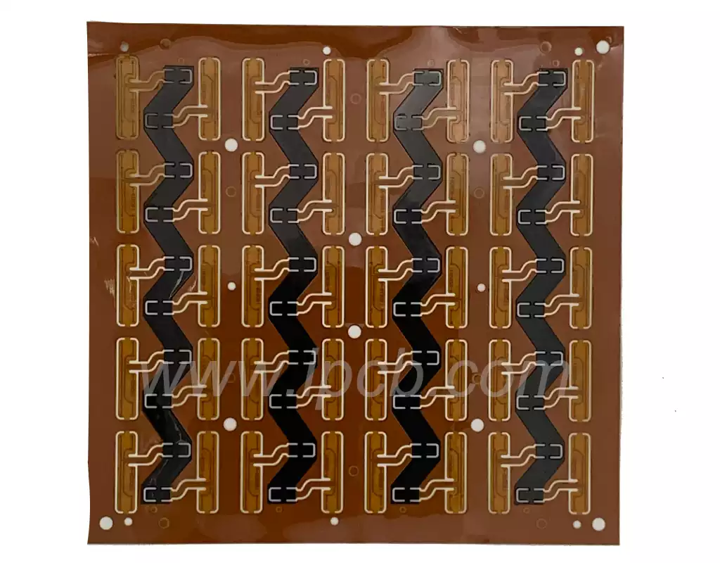
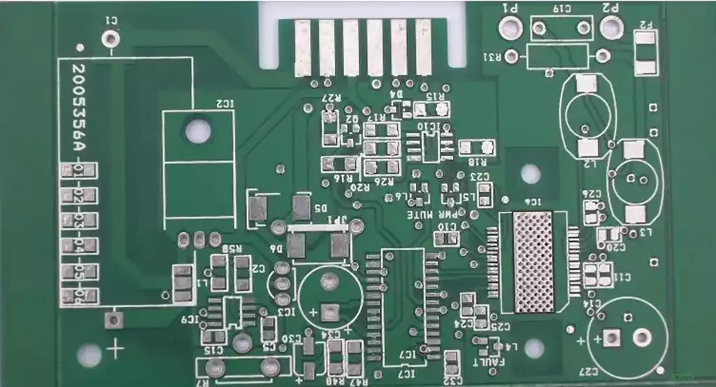
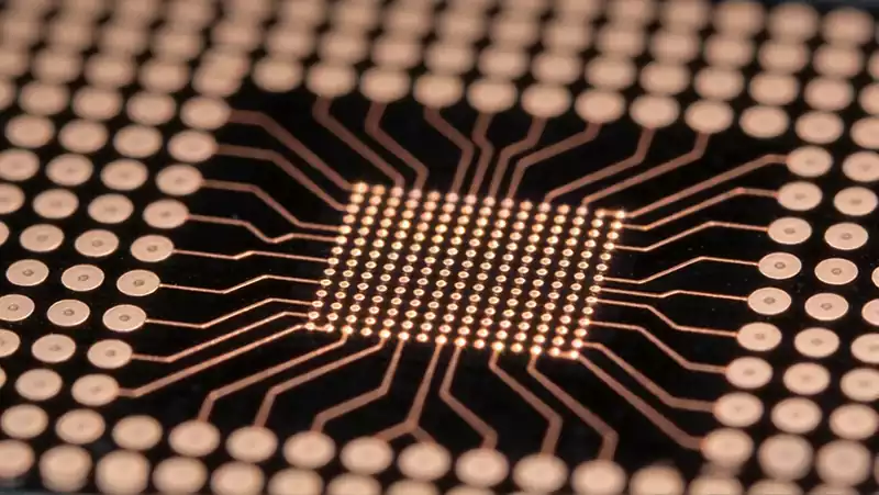
The boards play an important role in the manufacture of electronic equipment. As electronic devices become more complex and require more parts, the density of boards and assemblies continues to increase. Blank PCBs, also known as “Printed Circuit Boards”, have a substrate that is itself made of insulating and non-conductive material, while the small circuit material visible on the surface is copper. Originally, the entire board was covered with copper foil, but during the manufacturing process, some of the copper foil was etched away, leaving a network of tiny circuits to connect the components on the PCB.
Why is it important to test bare PCB? There are a number of reasons for this. As the basic framework of a circuit board, blank circuit boards can fail during the installation of wires and components, leading to a host of problems. Although failures are uncommon, the bare PCB board may already have defects before components are added. More common problems include over-etching, under-etching and holes. Even minor defects can lead to the failure of other manufacturing functions in the future, which can lead to more trouble. Therefore, quality checks are an essential part of the process to ensure that the circuit boards are up to snuff.
When blank printed circuit boards are used to make other circuit boards, the demand for multilayer PCB boards continues to grow as component density increases. This makes quality inspection of blank printed circuit boards even more critical. This is because it is virtually impossible to repair any failures that occur after the multilayer PCB is assembled. Assuming that the blank circuit board is faulty from the start, it amounts to a waste of time and manufacturing costs when manufacturing other boards in the future.
Timely testing of bare pcb brings many benefits. Don’t forget to check the blank circuit board for faults after it has been manufactured. This step can avoid many problems during the manufacturing process. Although the initial investment may be small, it can save a lot of maintenance and replacement costs. At the same time, testing of it helps to identify problems early in the manufacturing process. Identifying problems means finding the root cause of the problem and addressing the root cause. If the problem is discovered during the follow-up process, finding the root cause will become difficult. Once the component is covered on the PCB, it is impossible to determine the cause of the problem. Therefore, early testing helps eliminate the root cause.
In addition, testing simplifies the entire manufacturing process. If problems are identified and solved during the prototyping phase, the subsequent production phase can proceed smoothly.
With its simple design and flexible application, the blank PCB board offers the possibility of mass production and plays an important role in our daily life. From the basic to the application, a comprehensive understanding and mastery of the pcb substrate is undoubtedly an indispensable part of the electronic manufacturing field.