What is pcb warpage?Board warpage refers to the degree of surface bending and deformation of the circuit board, usually evaluated by two indicators, namely, the maximum warpage and the average warpage. The warpage of the circuit board will affect its use in practical applications, so it is very necessary to carry out strict control.
Standards for pcb warpage
At present, the international standards for circuit board warpage are IPC-6012, IPC-600 and J-STD-003. Among them, IPC-6012 is a more comprehensive circuit board manufacturing and assembly standards, which covers the circuit board manufacturing, quality management, design and testing and other aspects of the content of the circuit board warpage is also carried out in detail.
The IPC-6012 standard specifies a range of maximum and average warpage, as well as limits on different laminate and material types, thicknesses, dimensions, etc. The standard also specifies a range of maximum and average warpage, as well as limits on different laminates and materials. In addition, the standard regulates the appearance, quality, and dimensional deviations of circuit boards. For companies manufacturing circuit boards, compliance with the IPC-6012 standard ensures that the boards produced are of consistent quality and meet industry requirements.
IPC-600 is also widely used in the domestic market. The standard is mainly used for inspection and verification of circuit board production, which covers the specification of circuit board dimensions, materials, ignition, interfaces, solder joints, appearance, and surface characteristics. In addition, the J-STD-003 standard is also a common standard for pcb board production and assembly, which also specifies test methods for thermal stress performance, heat resistance, and other aspects of circuit boards.
Causes of board warpage
- Physical factors:board warpage is related to the rigidity of its circuit board material, coefficient of elasticity, temperature effects, size and other factors.
- Processing factors: circuit board heating, pressure, drilling, fixing screws torque, welding, polishing and other processes in the processing efforts.
- External factors: manufacturing process, use of the environment, storage conditions, transportation and other external factors may also cause deformation of the circuit board, which in turn affects the degree of warpage.
PCB warping causes
1.PCB warping causes
(1) The weight of the board itself will lead to board depression deformation
General reflow oven is a chain driven circuit board in the reflow oven to move forward, that is, the board on both sides as a fulcrum to support the entire board.
If there is a heavy weight on the board, or the board size is too large, due to the amount of the board, there will be a depression in the center, resulting in the board bending.
2) The V-cut is too deep, resulting in warping at the V-cut on both sides
Basically, the V-Cut is the culprit that destroys the structure of the board, because the V-Cut cuts grooves in the original large sheet, so the V-Cut tends to warp.
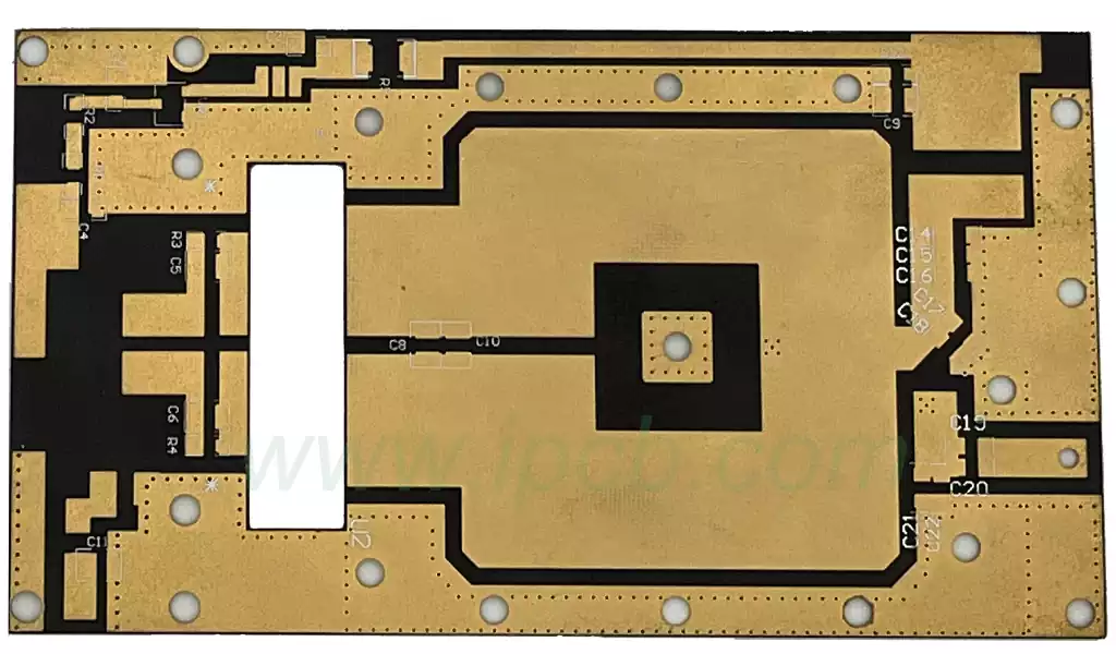
Influence of material, structure, and graphics on board warpage: PCBs are pressed from a core board, a semi-cured sheet, and an outer layer of copper foil. The core board and the copper foil will warp due to heat when pressed together. The amount of warpage depends on the coefficient of thermal expansion (CTE) of the two materials.
The coefficient of thermal expansion (CTE) of copper foil is about 17X10-6; while the Z-direction CTE of common FR-4 substrate under Tg point is (5070)X10-6; above TG point is (250350)X10-6, and X-direction CTE is generally similar to that of copper foil due to the existence of glass cloth.
- PCB processing process caused by warpage
PCB processing warpage cause is very complex, can be divided into thermal stress and mechanical stress.
Among them, thermal stress is mainly generated in the pressing process, and mechanical stress is mainly generated in the stacking, handling and baking process of the board.
(1) PCB warpage caused by incoming copper-clad board process
Copper cladding boards are all double-sided, symmetrical structure, no graphics. The CTE of copper foil and glass cloth are almost the same, so there is almost no warpage caused by different CTE in the pressing process.
However, the size of the copper-clad plate press is large, and the temperature difference between different areas of the hot plate can lead to slight differences in the resin curing speed and degree of curing in different areas during the press-fit process. At the same time, there are also large differences in dynamic viscosity at different rates of temperature rise, and thus localized stresses can also occur due to differences in the curing process.
Generally this stress will remain in equilibrium after pressing, but will be gradually released and deformed in the subsequent processing.
(2) PCB warpage caused by the PCB pressing process
PCB pressing process is the main process of generating thermal stress. Similar to the pressing of copper-clad laminates, localized stresses are also generated due to different curing processes. Thermal stresses can be more difficult to eliminate than in copper-clad boards due to thicker thicknesses, varied pattern distribution, and more prepreg.
The stresses in the PCB are released in the subsequent drilling, molding or grilling process, resulting in board deformation.
(3) PCB warpage caused by soldermask and silkscreen baking process
Due to the curing process in the soldermask ink can not be stacked on top of each other, the PCB board will be placed in the rack in the baking board curing.
Soldermask temperature of about 150 ℃, more than the Tg value of the copper-clad board, PCB is easy to soften resulting in can not withstand high temperatures. The builder must evenly heat both sides of the substrate, while keeping the processing time as short as possible to minimize the warpage of the substrate.
(4) PCB cooling and heating process caused by PCB warpage
Tin furnace temperature 225 ° C – 265 ° C, ordinary board hot air solder leveling time 3s – 6s. hot air temperature of 280 ° C – 300 ° C.
After solder leveling, the board from room temperature into the tin furnace, out of the two minutes after the normal temperature post-treatment washing. The whole hot air solder leveling process is a sudden heating and cooling process.
Due to the different materials and uneven structure of the circuit board, thermal stress will inevitably occur during the cooling and heating process, resulting in micro-strain and overall deformation of the warped area.
(5) PCB warpage caused by improper storage
PCB boards in the semi-finished stage of storage, are generally firmly inserted in the shelves, the tightness of the shelves are not adjusted, or the storage process of the board stacking will lead to mechanical deformation of the board.
Especially the thin boards below 2.0mm, the impact is more serious.
- Reasons for engineering design
The copper surface area on the circuit board is not uniform, more on one side and less on the other. Where the lines are sparse, the surface tension will be weaker than where it is dense, and too high a temperature will cause the board to warp.
The laminate structure may be asymmetrical due to special dielectric or impedance relationships, causing the board to warp.
The board itself has too many and many skeletonized locations, which are prone to warpage when the temperature is too high.
Too many panels on the board with hollow spacing between panels, especially rectangular boards, are also prone to warpage.
PCB warpage solution
- Check the design and materials: Make sure that proper support structures are considered in the PCB design and that appropriate boards are selected.
- Thermal management: Pay attention to thermal management during PCB manufacturing.
- Package selection: It is also important to select the correct package.
- Optimize layout: Reasonable layout of PCB components and circuits to avoid large heat sources or weight concentrated in one area.
- Structural reinforcement: Install reinforcement materials on the PCB to increase its stability and prevent warping.
- Fine assembly: Pay attention to the flatness and tightness of the patches in the assembly process.
- Temperature management: Control the PCB’s operating temperature to reduce the risk of warpage.
Board warpage control of circuit boards is an important part of ensuring product quality. We should effectively reduce the warpage phenomenon to improve the reliability and stability of the circuit board. Warpage control will continue to be optimized as technology continues to advance.