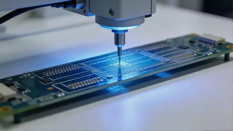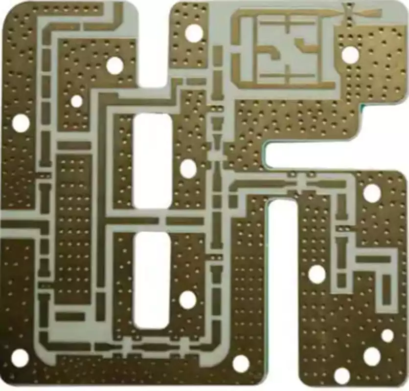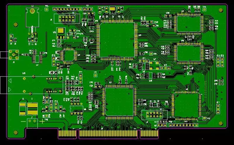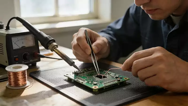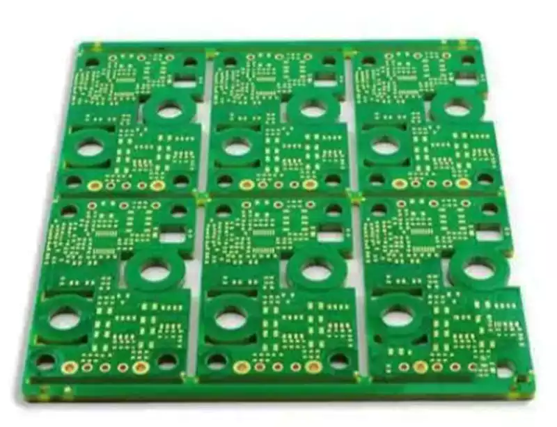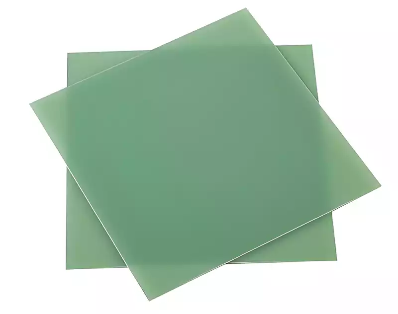
Rogers PCB High-Frequency Soldering Process
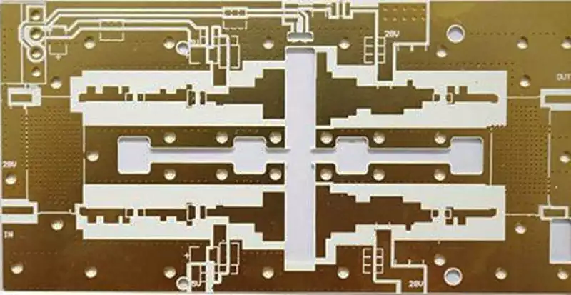
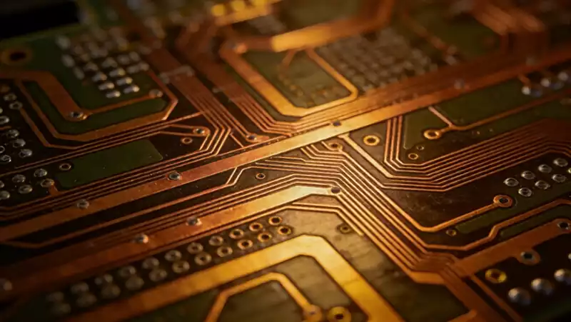
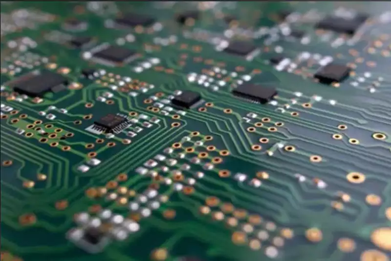
In the manufacture of RF and microwave circuits, Rogers PCBs serve as the core substrate due to their low dielectric loss and high dielectric stability. As the critical process for connecting components to the PCB, the soldering process directly determines the product’s signal integrity and long-term reliability. Unlike conventional FR4 boards, the special materials used […]